Wafer Level Packaging offers a cost-effective solution by packaging all dies on a wafer simultaneously, enabling thinner, smaller, and higher-performing semiconductor devices compared to Die Level Packaging, which packages individual dies separately, often resulting in increased assembly complexity and size. Understanding these differences helps you choose the optimal packaging method to enhance device reliability and manufacturing efficiency.
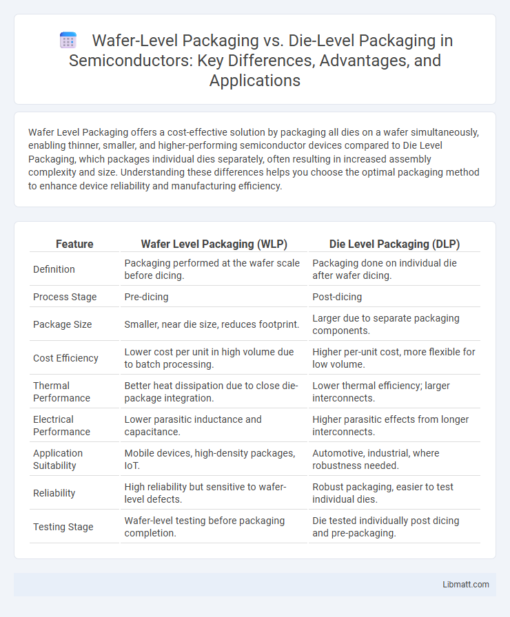
Table of Comparison
| Feature | Wafer Level Packaging (WLP) | Die Level Packaging (DLP) |
|---|---|---|
| Definition | Packaging performed at the wafer scale before dicing. | Packaging done on individual die after wafer dicing. |
| Process Stage | Pre-dicing | Post-dicing |
| Package Size | Smaller, near die size, reduces footprint. | Larger due to separate packaging components. |
| Cost Efficiency | Lower cost per unit in high volume due to batch processing. | Higher per-unit cost, more flexible for low volume. |
| Thermal Performance | Better heat dissipation due to close die-package integration. | Lower thermal efficiency; larger interconnects. |
| Electrical Performance | Lower parasitic inductance and capacitance. | Higher parasitic effects from longer interconnects. |
| Application Suitability | Mobile devices, high-density packages, IoT. | Automotive, industrial, where robustness needed. |
| Reliability | High reliability but sensitive to wafer-level defects. | Robust packaging, easier to test individual dies. |
| Testing Stage | Wafer-level testing before packaging completion. | Die tested individually post dicing and pre-packaging. |
Introduction to Semiconductor Packaging Technologies
Wafer Level Packaging (WLP) and Die Level Packaging (DLP) represent two pivotal semiconductor packaging technologies essential for protecting and interconnecting integrated circuits. WLP enables packaging directly at the wafer scale, improving performance, miniaturization, and manufacturing efficiency, while DLP involves packaging individual dies after wafer dicing, offering flexibility in handling and testing. Understanding these techniques enhances your ability to select optimal packaging suited for different electronic applications, influencing device reliability and cost.
Overview of Wafer Level Packaging (WLP)
Wafer Level Packaging (WLP) integrates packaging processes directly on the wafer before dicing, enabling smaller package sizes and enhanced electrical performance compared to traditional Die Level Packaging (DLP). WLP offers improved signal integrity, reduced parasitic elements, and superior thermal management by encapsulating and interconnecting multiple devices on the wafer scale. This technology supports advanced applications in smartphones, IoT devices, and high-frequency electronics where miniaturization and reliability are critical.
Overview of Die Level Packaging (DLP)
Die Level Packaging (DLP) involves individually packaging semiconductor dies after wafer dicing, enhancing flexibility in selecting specific chips for assembly. This method provides improved electrical performance and thermal management by tailoring packages to individual die needs. DLP supports heterogeneous integration and is commonly used in applications requiring high-performance and customized packaging solutions.
Core Differences: Wafer Level vs Die Level Packaging
Wafer Level Packaging (WLP) involves packaging integrated circuits directly at the wafer stage, enabling higher input/output (I/O) density and reduced package size compared to Die Level Packaging (DLP), which packages individual dies after wafer dicing. WLP offers enhanced electrical performance and thermal management due to shorter interconnects, while DLP provides flexibility in handling diverse die sizes and enables use in complex multi-die assemblies. The core difference lies in WLP's efficiency in miniaturization and throughput versus DLP's adaptability to varied package designs and post-fabrication testing.
Advantages of Wafer Level Packaging
Wafer Level Packaging (WLP) offers significant advantages such as reduced package size and improved electrical performance due to shorter interconnects compared to Die Level Packaging (DLP). This technology enhances thermal management and reliability by integrating packaging processes at the wafer scale, enabling higher throughput and lower production costs. Your designs benefit from the scalability and superior miniaturization that WLP provides, ideal for advanced semiconductor applications.
Benefits and Limitations of Die Level Packaging
Die Level Packaging offers precise individual chip protection and testing, enhancing yield and reliability by isolating defects at the die stage. This approach enables flexible customization and improved thermal management, making it ideal for high-performance applications requiring tailored solutions. However, the increased handling and assembly complexity can raise manufacturing costs and reduce throughput compared to Wafer Level Packaging.
Performance and Reliability Comparison
Wafer Level Packaging (WLP) offers superior electrical performance due to shorter interconnects and reduced parasitic inductance compared to Die Level Packaging (DLP), enhancing signal integrity and power efficiency. WLP also provides higher reliability under thermal cycling and mechanical stress, as the package is formed directly on the wafer, minimizing defects and improving thermal dissipation. Your choice between WLP and DLP impacts device longevity and performance, with WLP being ideal for high-frequency and miniaturized applications requiring robust reliability.
Cost Implications and Manufacturing Efficiency
Wafer Level Packaging (WLP) significantly reduces manufacturing costs by enabling simultaneous processing of multiple dies directly on the wafer, minimizing material waste and assembly steps compared to Die Level Packaging (DLP). DLP often incurs higher costs due to individual die handling, testing, and packaging, increasing labor and equipment expenses. WLP enhances manufacturing efficiency by streamlining processes and offering higher throughput rates, while DLP's flexibility serves niche applications with complex or varied package requirements but at the expense of longer production cycles.
Key Applications and Industry Adoption
Wafer Level Packaging (WLP) excels in compact consumer electronics and mobile devices due to its ability to enhance performance while minimizing package size. Die Level Packaging (DLP) is preferred in automotive, aerospace, and industrial sectors where robustness and thermal management are critical. Your choice between WLP and DLP should consider the application's space constraints, reliability requirements, and industry-specific adoption trends.
Future Trends in Semiconductor Packaging Technologies
Wafer Level Packaging (WLP) is advancing with trends like fan-out WLP and heterogeneous integration, enabling higher I/O density, miniaturization, and improved thermal performance, positioning it as a key technology for next-generation smartphones and IoT devices. Die Level Packaging (DLP) continues to evolve through high-density interconnects and advanced substrate materials, supporting robust solutions for automotive and aerospace applications requiring enhanced reliability and performance. The future of semiconductor packaging sees converging innovations in 3D stacking, system-in-package (SiP), and advanced materials driving both WLP and DLP toward ultra-compact, high-performance, and energy-efficient devices in AI and 5G technology landscapes.
Wafer Level Packaging vs Die Level Packaging Infographic