Lapped wafers have a rougher surface finish achieved through coarse grinding, ideal for intermediate processing steps, while polished wafers feature an ultra-smooth, mirror-like surface essential for final semiconductor device fabrication. Your choice depends on the specific requirements for surface flatness and cleanliness in your semiconductor manufacturing process.
Table of Comparison
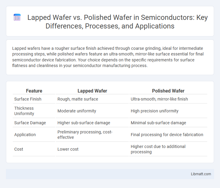
| Feature | Lapped Wafer | Polished Wafer |
|---|---|---|
| Surface Finish | Rough, matte surface | Ultra-smooth, mirror-like finish |
| Thickness Uniformity | Moderate uniformity | High precision uniformity |
| Surface Damage | Higher sub-surface damage | Minimal sub-surface damage |
| Application | Preliminary processing, cost-effective | Final processing for device fabrication |
| Cost | Lower cost | Higher cost due to additional processing |
Introduction to Semiconductor Wafers
Semiconductor wafers serve as the foundational substrate in microelectronics, with lapped wafers featuring a rougher surface that aids in material removal and thickness control during manufacturing. Polished wafers offer a mirror-smooth finish crucial for photolithography and device fabrication, enhancing semiconductor performance and yield. Understanding the distinctions between lapped and polished wafers helps optimize Your semiconductor processing for improved circuit reliability and efficiency.
What Is a Lapped Wafer?
A lapped wafer is a silicon substrate that undergoes a mechanical grinding process to achieve a flat surface with controlled thickness but retains a slightly rough texture compared to polished wafers. This process removes material from the wafer's backside or front side, improving wafer uniformity while maintaining surface integrity for subsequent fabrication steps. Lapped wafers are typically used in semiconductor device manufacturing where surface planarity is crucial but ultra-smooth finishes, characteristic of polished wafers, are not required.
What Is a Polished Wafer?
A polished wafer is a semiconductor substrate that has undergone chemical mechanical polishing (CMP) to achieve an ultra-smooth, defect-free surface essential for integrated circuit fabrication. This highly planar surface enhances photolithography resolution and ensures uniform thin film deposition, critical for advanced semiconductor devices. Compared to lapped wafers, which have a rougher surface from mechanical grinding, polished wafers offer superior surface quality and dimensional precision necessary for high-performance microelectronics.
Key Differences Between Lapped and Polished Wafers
Lapped wafers feature a rougher surface achieved through coarse abrasive grinding, while polished wafers undergo finer chemical-mechanical polishing to attain a mirror-like finish. The surface texture differences impact semiconductor device performance, with polished wafers providing improved flatness and reduced surface defects crucial for high-precision applications. Your choice between lapped and polished wafers depends on the balance between cost-efficiency and the required surface quality in semiconductor manufacturing.
Surface Quality and Flatness Comparison
Lapped wafers feature a rougher surface finish with higher surface defects compared to polished wafers, which exhibit superior smoothness and minimal surface irregularities critical for semiconductor device fabrication. The flatness of polished wafers is significantly enhanced due to precision chemical-mechanical planarization (CMP), achieving nanometer-scale planarity, whereas lapped wafers often show greater surface waviness and bowing defects. High flatness and surface quality in polished wafers are essential for advanced lithography and thin-film deposition processes, directly impacting yield and device performance.
Applications of Lapped Wafers
Lapped wafers, characterized by their controlled flatness and surface roughness, are ideal for applications requiring precise thickness control and mechanical durability, such as semiconductor device fabrication and MEMS (Micro-Electro-Mechanical Systems) manufacturing. These wafers serve as substrates in power electronics and sensor technologies where surface planarity impacts device performance but ultra-smooth polishing is not critical. Your choice of lapped wafers supports processes like epitaxial growth and thin-film deposition where uniform thickness and minimal surface damage are essential.
Applications of Polished Wafers
Polished wafers are essential in semiconductor manufacturing, providing a smooth, defect-free surface ideal for photolithography and thin-film deposition processes. Their precision surface finish enables high-performance integrated circuits, MEMS devices, and advanced microelectronic applications requiring tight dimensional control. You can rely on polished wafers for applications demanding superior surface quality and enhanced device reliability.
Cost Considerations: Lapped vs Polished Wafers
Lapped wafers offer a cost-effective solution by utilizing a less labor-intensive grinding process that reduces material waste and processing time compared to the more expensive and time-consuming polished wafer finishing, which requires precise chemical-mechanical planarization. Polished wafers provide superior surface quality essential for high-precision semiconductor applications, but the increased production costs make lapped wafers preferable for less critical uses or early-stage prototyping. Cost savings in lapped wafers stem from lower equipment wear and reduced use of expensive slurry and polishing pads, making them ideal when budget constraints outweigh the need for ultra-smooth surfaces.
Choosing the Right Wafer for Your Project
Choosing the right wafer for your project depends on surface quality and application requirements; lapped wafers offer a flat but rougher surface suitable for processes where perfect smoothness is not critical, while polished wafers provide ultra-smooth, mirror-like surfaces essential for high-precision semiconductor fabrication and optical applications. Polished wafers undergo extensive chemical and mechanical polishing to remove subsurface damage and achieve nanometer-scale flatness, which enhances device performance and yield. Selecting between lapped and polished wafers hinges on factors like processing steps, cost, and the need for surface uniformity and defect minimization.
Conclusion: Lapped vs Polished Wafer Selection
Lapped wafers offer a rougher surface ideal for preliminary processing steps where material removal and thickness control are critical, while polished wafers provide a smooth, defect-free surface essential for high-precision semiconductor applications. Selecting between lapped and polished wafers depends on the specific manufacturing stage and device requirements, balancing cost-effectiveness against surface quality demands. For final device fabrication, polished wafers are preferred due to their superior planarity and minimal surface defects that enhance device performance and yield.
Lapped Wafer vs Polished Wafer Infographic