Sputter deposition creates thin films by bombarding a target material with energetic particles, resulting in highly uniform coatings with excellent adhesion and precise thickness control. Evaporation involves heating a source material until it vaporizes and condenses onto a substrate, offering faster deposition rates but often less uniformity and weaker film adhesion compared to sputtering.
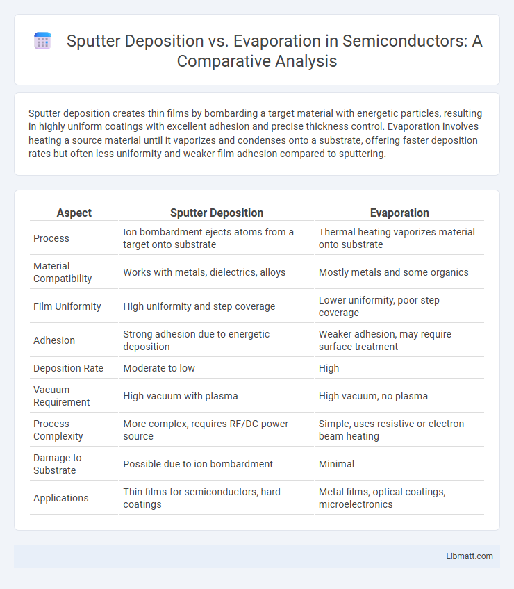
Table of Comparison
| Aspect | Sputter Deposition | Evaporation |
|---|---|---|
| Process | Ion bombardment ejects atoms from a target onto substrate | Thermal heating vaporizes material onto substrate |
| Material Compatibility | Works with metals, dielectrics, alloys | Mostly metals and some organics |
| Film Uniformity | High uniformity and step coverage | Lower uniformity, poor step coverage |
| Adhesion | Strong adhesion due to energetic deposition | Weaker adhesion, may require surface treatment |
| Deposition Rate | Moderate to low | High |
| Vacuum Requirement | High vacuum with plasma | High vacuum, no plasma |
| Process Complexity | More complex, requires RF/DC power source | Simple, uses resistive or electron beam heating |
| Damage to Substrate | Possible due to ion bombardment | Minimal |
| Applications | Thin films for semiconductors, hard coatings | Metal films, optical coatings, microelectronics |
Introduction to Thin Film Deposition Methods
Sputter deposition and evaporation are key thin film deposition methods used in semiconductor manufacturing and material sciences to create uniform, high-quality coatings. Sputter deposition involves ejecting atoms from a target material using energetic ion bombardment, enabling precise control over film composition and excellent adhesion on diverse substrates. Evaporation relies on thermal energy to vaporize materials, which then condense on a surface, offering high deposition rates but limited control over film uniformity and step coverage compared to sputtering.
Overview of Sputter Deposition
Sputter deposition is a physical vapor deposition (PVD) technique used to deposit thin films by ejecting atoms from a solid target material onto a substrate through ion bombardment. This method offers advantages such as excellent film adhesion, uniform coverage on complex surfaces, and the ability to deposit a wide range of materials including metals, insulators, and alloys. Its precise control over film thickness and composition makes sputter deposition ideal for semiconductor manufacturing, optical coatings, and magnetic storage devices.
Overview of Evaporation Techniques
Evaporation techniques in thin film deposition involve heating a source material until it vaporizes and condenses onto a substrate, commonly used for metals, oxides, and organic materials. Thermal evaporation and electron beam evaporation are primary methods, with thermal evaporation relying on resistive heating and electron beam evaporation utilizing focused electron beams to achieve higher temperatures and better control. These techniques excel in producing uniform, high-purity films but often require ultra-high vacuum conditions to minimize contamination and achieve precise film thickness.
Process Mechanisms: Sputtering vs. Evaporation
Sputter deposition uses ionized gas to bomb particles from a target material, creating a highly uniform and dense thin film with excellent adhesion to the substrate. Evaporation relies on heating the source material until it vaporizes, allowing atoms to condense onto the substrate, which may result in less control over film density and coverage uniformity. Your choice between sputtering and evaporation depends on the desired film properties, target materials, and substrate compatibility.
Material Compatibility and Flexibility
Sputter deposition offers broader material compatibility, effectively coating metals, oxides, and nitrides with strong adhesion and uniformity, while evaporation is often limited to materials with lower melting points. Sputtering enables greater flexibility in film composition through reactive gases and co-sputtering techniques, allowing precise control over film stoichiometry. Your choice depends on the required film properties, substrate sensitivity, and desired material versatility for the application.
Film Quality: Uniformity and Adhesion
Sputter deposition offers superior film uniformity and adhesion compared to evaporation due to its higher energy particle bombardment, which enhances film density and coverage on complex substrates. Your thin films benefit from sputtering's improved step coverage and reduced defects, ensuring consistent thickness across large areas. Evaporation may produce less uniform layers with weaker adhesion, particularly on uneven surfaces or when depositing metals prone to island growth.
Deposition Rate and Process Control
Sputter deposition offers precise process control with uniform thin films due to its ionized particle generation, but typically has a slower deposition rate compared to evaporation methods. Evaporation techniques achieve higher deposition rates by vaporizing source material directly, though they may sacrifice uniformity and control over film thickness. Your choice depends on prioritizing faster deposition or superior process control for applications like microelectronics or optical coatings.
Equipment Complexity and Cost
Sputter deposition systems involve more complex equipment, including plasma generators, gas delivery, and target materials, leading to higher initial capital and maintenance costs compared to evaporation systems. Evaporation employs simpler thermal or electron beam sources, resulting in lower equipment complexity and reduced operational expenses. The enhanced control and uniformity from sputtering justify its cost in high-precision thin-film applications.
Applications and Industry Preferences
Sputter deposition is widely preferred in microelectronics and hard coating industries due to its uniform film thickness, high adhesion, and ability to deposit complex alloys. Evaporation finds extensive use in optical coatings and decorative finishes where high deposition rates and simpler equipment are advantageous. Your choice between sputtering and evaporation depends on specific application requirements such as film quality, material type, and production scale.
Choosing the Right Method: Key Considerations
Sputter deposition offers superior film adhesion and uniformity, making it ideal for complex surface geometries, while evaporation provides higher deposition rates and purity suited for simpler, line-of-sight applications. Your choice depends on factors such as substrate material, desired film thickness, and the complexity of the pattern required. Evaluating these parameters ensures optimal coating performance and process efficiency.
Sputter Deposition vs Evaporation Infographic