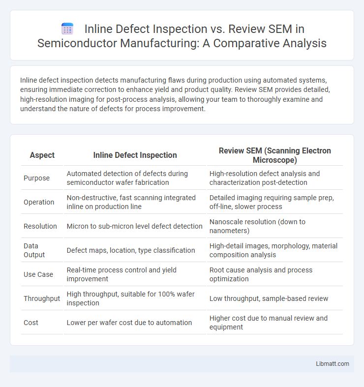
Inline defect inspection detects manufacturing flaws during production using automated systems, ensuring immediate correction to enhance yield and product quality. Review SEM provides detailed, high-resolution imaging for post-process analysis, allowing your team to thoroughly examine and understand the nature of defects for process improvement.
Table of Comparison
| Aspect | Inline Defect Inspection | Review SEM (Scanning Electron Microscope) |
|---|---|---|
| Purpose | Automated detection of defects during semiconductor wafer fabrication | High-resolution defect analysis and characterization post-detection |
| Operation | Non-destructive, fast scanning integrated inline on production line | Detailed imaging requiring sample prep, off-line, slower process |
| Resolution | Micron to sub-micron level defect detection | Nanoscale resolution (down to nanometers) |
| Data Output | Defect maps, location, type classification | High-detail images, morphology, material composition analysis |
| Use Case | Real-time process control and yield improvement | Root cause analysis and process optimization |
| Throughput | High throughput, suitable for 100% wafer inspection | Low throughput, sample-based review |
| Cost | Lower per wafer cost due to automation | Higher cost due to manual review and equipment |
Understanding Inline Defect Inspection
Inline Defect Inspection involves real-time monitoring and detection of manufacturing flaws on semiconductor wafers during the production process, enabling immediate identification and correction of defects. This method utilizes advanced imaging techniques such as optical and electron microscopy directly integrated into the production line, ensuring higher throughput and reduced downtime. Understanding Inline Defect Inspection is critical for improving yield, maintaining quality control, and minimizing costly rework in semiconductor manufacturing.
What Is Review SEM?
Review SEM (Scanning Electron Microscopy) is a high-resolution imaging technique used to analyze semiconductor wafers for defects after initial Inline Defect Inspection identifies potential issues. It provides detailed topographical and compositional information at the nanoscale, enabling precise characterization of defects that impact yield and device performance. You rely on Review SEM to validate inline inspection results and guide process improvements through thorough defect analysis.
Key Differences Between Inline Defect Inspection and Review SEM
Inline Defect Inspection focuses on real-time detection of defects during semiconductor manufacturing, enabling immediate process adjustments to prevent yield loss and enhance production efficiency. Review SEM (Scanning Electron Microscopy), by contrast, is used for detailed post-process analysis, providing high-resolution imaging and measurements to identify failure mechanisms and root causes of defects. Your choice depends on whether you need rapid feedback to control manufacturing or in-depth analysis for quality assurance and process optimization.
Advantages of Inline Defect Inspection
Inline Defect Inspection offers real-time monitoring and immediate identification of manufacturing defects, significantly reducing wafer scrap rates and improving yield efficiency in semiconductor fabrication. This method enables faster feedback loops compared to Review SEM, which is primarily used for detailed post-process analysis, leading to enhanced production throughput and cost savings. By integrating inspections directly into the production line, Inline Defect Inspection supports continuous process control and quicker corrective actions, optimizing overall semiconductor device quality.
Benefits of Review SEM in Semiconductor Manufacturing
Review SEM enhances semiconductor manufacturing by providing high-resolution imaging that precisely identifies nanoscale defects missed during inline defect inspection. This technique allows for detailed analysis of failure mechanisms, enabling targeted corrective actions and reducing overall production yield loss. By using Review SEM, your process control improves, accelerating root cause identification and enhancing product reliability.
Limitations of Inline Defect Inspection
Inline Defect Inspection faces limitations such as lower resolution compared to Review Scanning Electron Microscopy (SEM), hindering its ability to accurately identify sub-micron defects. The inline process often struggles with complex topographies and dense patterns, leading to false positives or missed defects. These constraints reduce its effectiveness in detecting critical flaws, necessitating supplementary use of Review SEM for detailed failure analysis.
Challenges Associated with Review SEM
Review Scanning Electron Microscopy (SEM) faces challenges such as limited throughput and increased analysis time compared to Inline Defect Inspection systems, which can slow down semiconductor manufacturing processes. The complexity of sample preparation and operator expertise requirements in Review SEM often lead to bottlenecks in defect characterization and root cause analysis. Your ability to maintain high production efficiency depends on balancing detailed defect insights from Review SEM with the speed and automation offered by Inline Defect Inspection.
Application Scenarios: When to Use Each Method
Inline Defect Inspection is ideal for real-time monitoring and immediate quality control during semiconductor manufacturing, helping to quickly identify and address defects on wafers to minimize production downtime. Review SEM excels in detailed analysis and characterization of defects after fabrication, providing high-resolution imaging essential for failure analysis and root cause identification. Your choice depends on whether you need rapid defect detection during production or in-depth understanding of defect morphology for process improvement.
Integrating Inline Defect Inspection and Review SEM in Workflow
Integrating Inline Defect Inspection (IDI) with Review Scanning Electron Microscopy (SEM) enhances semiconductor manufacturing by combining real-time defect detection with detailed defect characterization. This workflow integration enables faster root cause analysis and improves yield by linking inline inspection data to high-resolution SEM images for accurate defect classification. Leveraging advanced data correlation and automation tools facilitates seamless communication between IDI systems and SEM review stations, optimizing production efficiency and defect management.
Future Trends in Defect Detection Technologies
Inline defect inspection is evolving with advances in AI-driven image analysis and real-time data processing, enabling faster identification and classification of microscopic defects during semiconductor manufacturing. Review SEM (Scanning Electron Microscopy) is integrating enhanced automation and machine learning to improve resolution and defect characterization accuracy for post-process analysis. Future trends emphasize the convergence of inline inspection and review SEM technologies, leveraging hybrid systems for comprehensive defect detection that reduces production downtime and improves yield management.
Inline Defect Inspection vs Review SEM Infographic