Photolithography offers high throughput and cost-efficiency for mass production of microchips but is limited by optical resolution constraints, making it less suitable for features below 10 nanometers. Electron Beam Lithography provides superior resolution and flexibility for creating nanoscale patterns, ideal for research and prototyping, though it is slower and more expensive, impacting your production speed and budget.
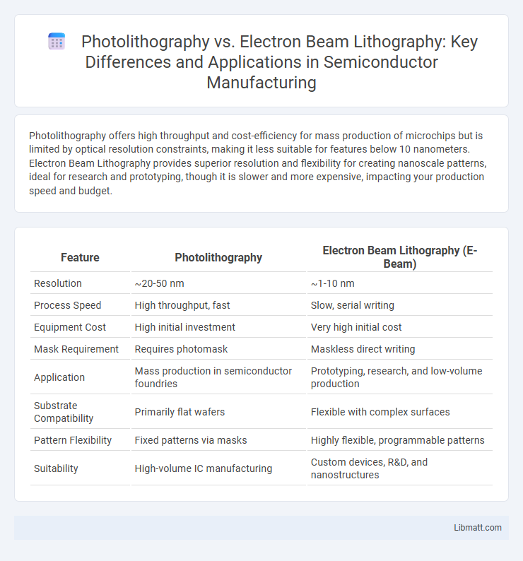
Table of Comparison
| Feature | Photolithography | Electron Beam Lithography (E-Beam) |
|---|---|---|
| Resolution | ~20-50 nm | ~1-10 nm |
| Process Speed | High throughput, fast | Slow, serial writing |
| Equipment Cost | High initial investment | Very high initial cost |
| Mask Requirement | Requires photomask | Maskless direct writing |
| Application | Mass production in semiconductor foundries | Prototyping, research, and low-volume production |
| Substrate Compatibility | Primarily flat wafers | Flexible with complex surfaces |
| Pattern Flexibility | Fixed patterns via masks | Highly flexible, programmable patterns |
| Suitability | High-volume IC manufacturing | Custom devices, R&D, and nanostructures |
Introduction to Photolithography and Electron Beam Lithography
Photolithography uses ultraviolet light to transfer geometric patterns onto a photosensitive resist, enabling high-throughput semiconductor manufacturing with precise feature sizes typically down to 20 nanometers. Electron Beam Lithography (EBL) employs a focused electron beam to directly write patterns on the resist, offering superior resolution at the sub-10 nanometer scale but with slower throughput and higher costs. You can choose photolithography for mass production and electron beam lithography for research or prototyping requiring ultra-fine features.
Fundamental Principles of Each Technique
Photolithography uses ultraviolet light to transfer geometric patterns from a photomask onto a photoresist-coated substrate, relying on light diffraction for pattern resolution. Electron beam lithography (EBL) directs a focused electron beam to precisely write patterns onto an electron-sensitive resist, enabling nanometer-scale resolution without the need for masks. Your choice between these techniques depends on required feature size, throughput, and pattern complexity, with photolithography suited for high-volume production and EBL ideal for prototyping and high-precision applications.
Process Workflow: Step-by-Step Comparison
Photolithography begins with substrate cleaning, photoresist application, mask alignment, UV light exposure, and development to create patterns on the wafer surface. Electron Beam Lithography (EBL) skips masks by directly writing patterns with a focused electron beam, followed by resist development and substrate etching. While photolithography offers faster throughput and cost-effectiveness for large volume production, EBL provides higher resolution and design flexibility at the expense of longer processing times and higher operational costs.
Resolution and Patterning Capabilities
Electron Beam Lithography (EBL) offers superior resolution down to sub-10 nanometers, enabling the creation of highly precise and complex nanoscale patterns unattainable by Photolithography, which typically achieves feature sizes around 100 nanometers. Photolithography excels in high-throughput patterning for large-scale semiconductor manufacturing but is limited by diffraction effects and the wavelength of light used. EBL's direct-write capability allows for versatile patterning without masks, making it ideal for prototyping and research despite slower processing speeds.
Throughput and Production Efficiency
Photolithography offers significantly higher throughput compared to Electron Beam Lithography (EBL) due to its parallel processing capabilities, making it ideal for large-scale semiconductor manufacturing. Electron Beam Lithography, while providing superior resolution for nanoscale patterning, operates at a slower serial writing speed that limits its production efficiency in high-volume environments. Your choice between these technologies should balance the need for resolution precision against throughput requirements in your manufacturing process.
Material Compatibility and Substrate Options
Photolithography primarily supports silicon wafers and organic photoresists, offering high throughput for semiconductor manufacturing but limited compatibility with diverse materials such as flexible substrates or non-planar surfaces. Electron Beam Lithography (EBL) excels in material compatibility, enabling patterning on a wider range of substrates including metals, polymers, and insulators, with exceptional precision at the nanoscale. By choosing EBL, Your processes can leverage greater substrate versatility and address complex material integration challenges not feasible with traditional photolithography.
Cost Considerations and Equipment Investment
Photolithography typically involves lower initial equipment costs and faster processing times, making it more cost-effective for high-volume semiconductor manufacturing. Electron Beam Lithography requires significant investment in specialized vacuum systems and electron sources, resulting in higher expenses suited for low-volume, high-precision applications such as prototyping and research. Your choice depends on balancing budget constraints with the need for resolution and throughput in device fabrication.
Applications in Microfabrication and Nanotechnology
Photolithography is widely used in microfabrication for producing semiconductor devices, microelectromechanical systems (MEMS), and integrated circuits due to its high throughput and capability to pattern features down to sub-100 nanometers. Electron beam lithography offers superior resolution reaching below 10 nanometers, making it essential for advanced nanotechnology applications such as prototype development, nanopatterning, and fabricating quantum devices where precise nanoscale control is critical. The choice between photolithography and electron beam lithography is determined by the required feature size, throughput, and application complexity in micro and nano fabrication processes.
Advantages and Limitations of Each Method
Photolithography offers high throughput and cost-effectiveness for mass production of semiconductor devices, with feature sizes typically down to 7 nm using extreme ultraviolet (EUV) wavelengths, but struggles with resolution limits imposed by light diffraction and mask costs. Electron beam lithography (EBL) provides unparalleled precision and flexibility in patterning sub-10 nm features, crucial for research and prototype development, yet its low throughput and higher operational costs restrict its use to small-scale fabrication. While photolithography excels in volume manufacturing due to scalability, EBL is favored for custom, high-resolution applications where intricate patterning outweighs speed constraints.
Future Developments and Industry Trends
Photolithography is advancing with extreme ultraviolet (EUV) light sources improving resolution for mass semiconductor production, while electron beam lithography (EBL) focuses on enhancing beam control and throughput for niche applications like quantum devices and prototype fabrication. The semiconductor industry trends toward hybrid lithography approaches integrating both technologies to balance cost-efficiency and precision, addressing the escalating demands of node scaling beyond 3 nm. Your choice of lithography method will depend on trade-offs between throughput, resolution, and application-specific requirements as these future developments shape manufacturing capabilities.
Photolithography vs Electron Beam Lithography Infographic