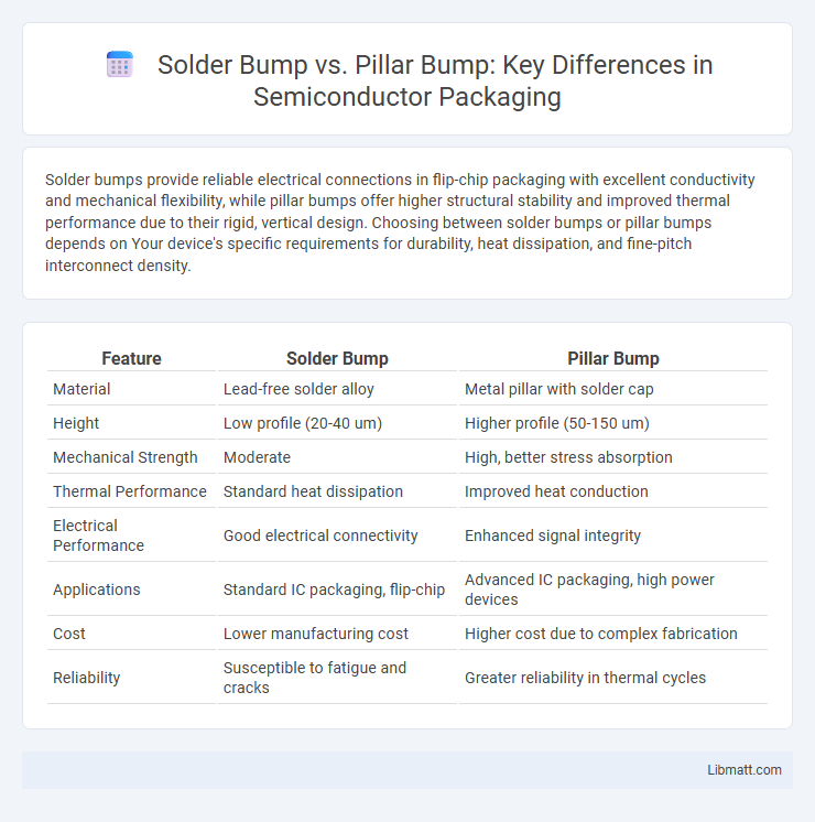
Solder bumps provide reliable electrical connections in flip-chip packaging with excellent conductivity and mechanical flexibility, while pillar bumps offer higher structural stability and improved thermal performance due to their rigid, vertical design. Choosing between solder bumps or pillar bumps depends on Your device's specific requirements for durability, heat dissipation, and fine-pitch interconnect density.
Table of Comparison
| Feature | Solder Bump | Pillar Bump |
|---|---|---|
| Material | Lead-free solder alloy | Metal pillar with solder cap |
| Height | Low profile (20-40 um) | Higher profile (50-150 um) |
| Mechanical Strength | Moderate | High, better stress absorption |
| Thermal Performance | Standard heat dissipation | Improved heat conduction |
| Electrical Performance | Good electrical connectivity | Enhanced signal integrity |
| Applications | Standard IC packaging, flip-chip | Advanced IC packaging, high power devices |
| Cost | Lower manufacturing cost | Higher cost due to complex fabrication |
| Reliability | Susceptible to fatigue and cracks | Greater reliability in thermal cycles |
Introduction to Solder Bump and Pillar Bump Technologies
Solder bump technology utilizes small spheres of solder alloy to create electrical connections in semiconductor packaging, offering excellent electrical conductivity and mechanical flexibility. Pillar bump technology, in contrast, employs metal pillars, often copper with a solder cap, to provide enhanced structural support and improved thermal performance in high-density interconnects. Both technologies are critical in advanced packaging, with solder bumps favored for traditional flip-chip applications and pillar bumps increasingly adopted for next-generation high-reliability and fine-pitch designs.
Historical Evolution of Bump Technologies in Electronics
Solder bump technology, originating in the 1980s, revolutionized microelectronic packaging by enabling flip-chip mounting with reliable electrical and mechanical connections. Pillar bump technology, developed in the 2000s, emerged to address the limitations of solder bumps, such as electromigration and thermal stress, by providing enhanced mechanical robustness and finer pitch capabilities for advanced semiconductor devices. The evolution from solder bumps to pillar bumps reflects the industry's demand for higher performance, miniaturization, and improved reliability in complex integrated circuits.
Structural Differences: Solder Bump vs Pillar Bump
Solder bumps consist primarily of a spherical metal alloy, typically tin-lead or lead-free solder, forming a simple, rounded connection point between semiconductor dies and substrates. Pillar bumps feature a more complex structure with a metal pillar, usually copper or nickel, topped by a solder cap, providing enhanced mechanical strength and finer pitch capabilities. The rigid metal pillar in pillar bumps offers superior resistance to thermal and mechanical stresses compared to the softer, purely solder-based solder bumps.
Fabrication Processes: Step-by-Step Comparison
Solder bump fabrication involves depositing a solder alloy onto the wafer pad, followed by reflow to form a hemispherical shape, often using electroplating or screen printing methods. Pillar bump fabrication starts with creating a metal pillar through electroplating, followed by capping with solder or protective plating to improve reliability and electromigration resistance. The solder bump process emphasizes simplicity and lower cost, while the pillar bump process offers enhanced mechanical strength and finer pitch capabilities through more complex, multi-step fabrication.
Material Selection: Alloys and Metals Used
Solder bumps typically use tin-based alloys such as SnAgCu (tin-silver-copper) or SnPb (tin-lead) for reliable electrical conductivity and mechanical flexibility. Pillar bumps often incorporate copper or nickel core materials plated with solder or gold to enhance strength and thermal performance in advanced packaging. Your choice between solder bump and pillar bump materials impacts joint reliability, thermal cycling tolerance, and overall packaging integrity.
Electrical Performance: Signal Integrity and Resistance
Solder bumps exhibit lower electrical resistance and superior signal integrity due to their smaller size and uniform contact area, making them ideal for high-frequency applications. Pillar bumps, while slightly larger, provide enhanced mechanical stability but may introduce higher resistance and potential signal degradation in ultra-high-speed circuits. Optimizing bump geometry and materials is essential to balance signal integrity and resistance for reliable semiconductor package performance.
Mechanical Reliability and Stress Management
Solder bumps offer excellent mechanical compliance due to their inherent ductility, effectively absorbing thermal stress and reducing deformation risks in microelectronic packaging. Pillar bumps, constructed from solid metal structures like copper or nickel, provide superior mechanical reliability under high-stress conditions by minimizing plastic deformation and enhancing fatigue resistance. Your choice depends on balancing flexibility for stress management with the need for robust mechanical endurance in demanding applications.
Application Areas: Where Each Bump Excels
Solder bumps excel in traditional flip-chip packaging for consumer electronics, offering reliable electrical connections and efficient heat dissipation in high-volume production. Pillar bumps are preferred in advanced packaging applications like 3D ICs and high-frequency devices, providing superior mechanical strength and better control over bump height for improved signal integrity. Your choice depends on whether the application demands cost-effective mass production or enhanced performance in complex, high-density integrations.
Cost Efficiency and Manufacturing Scalability
Solder bumps offer lower cost efficiency due to simpler materials and processes, making them ideal for high-volume manufacturing with established infrastructure. Pillar bumps, while more expensive upfront, provide superior manufacturing scalability through enhanced mechanical strength and reliability, reducing failure rates in complex semiconductor packaging. You benefit from choosing solder bumps for budget-sensitive applications and pillar bumps when long-term performance and scalability are critical.
Future Trends and Innovations in Bump Technology
Solder bump technology is evolving with the integration of lead-free alloys and nano-solder materials to enhance electrical performance and reliability in advanced semiconductor packaging. Pillar bump innovations emphasize fine-pitch scaling and improved mechanical strength using copper pillars with solder caps, supporting higher I/O density and thermal dissipation for next-generation devices. Emerging trends in bump technology include hybrid bump structures that combine solder and pillar features to optimize electrical conductivity, mechanical stability, and miniaturization in 3D IC integration and heterogeneous packaging.
Solder Bump vs Pillar Bump Infographic