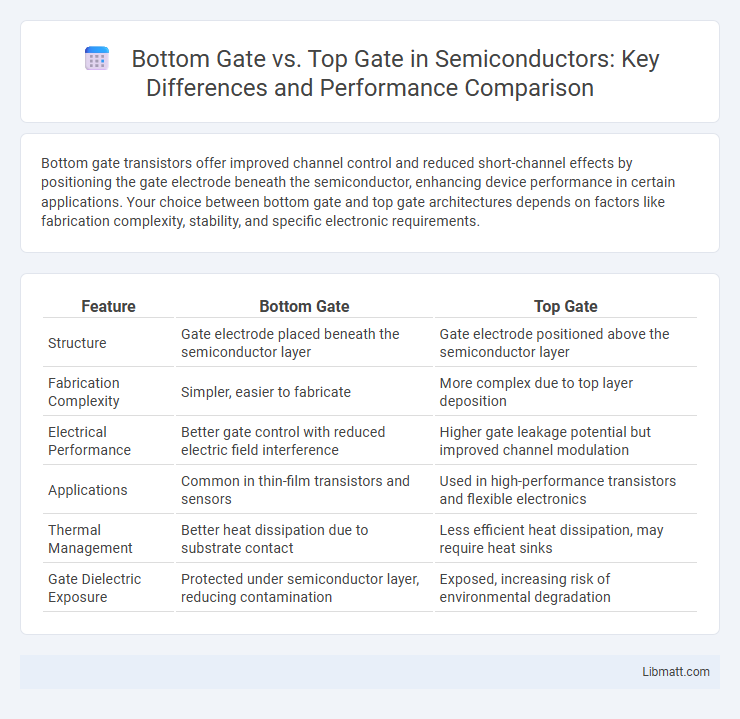
Bottom gate transistors offer improved channel control and reduced short-channel effects by positioning the gate electrode beneath the semiconductor, enhancing device performance in certain applications. Your choice between bottom gate and top gate architectures depends on factors like fabrication complexity, stability, and specific electronic requirements.
Table of Comparison
| Feature | Bottom Gate | Top Gate |
|---|---|---|
| Structure | Gate electrode placed beneath the semiconductor layer | Gate electrode positioned above the semiconductor layer |
| Fabrication Complexity | Simpler, easier to fabricate | More complex due to top layer deposition |
| Electrical Performance | Better gate control with reduced electric field interference | Higher gate leakage potential but improved channel modulation |
| Applications | Common in thin-film transistors and sensors | Used in high-performance transistors and flexible electronics |
| Thermal Management | Better heat dissipation due to substrate contact | Less efficient heat dissipation, may require heat sinks |
| Gate Dielectric Exposure | Protected under semiconductor layer, reducing contamination | Exposed, increasing risk of environmental degradation |
Introduction to Bottom Gate and Top Gate Technologies
Bottom gate and top gate technologies refer to the placement of the gate electrode in thin-film transistors (TFTs), a key component in modern display and sensor applications. Bottom gate structures position the gate electrode beneath the semiconductor layer, offering ease of fabrication and compatibility with various substrates, while top gate designs place the gate electrode above the semiconductor, providing better channel control and reduced parasitic capacitance. Your choice between these technologies depends on factors like device performance, fabrication complexity, and intended application requirements.
Key Differences Between Bottom Gate and Top Gate Structures
Bottom gate structures position the gate electrode beneath the semiconductor layer, offering improved substrate compatibility and reduced parasitic capacitance, which enhances device performance in flexible electronics. Top gate configurations place the gate electrode above the semiconductor, enabling better channel control and higher carrier mobility, often preferred in thin-film transistors for displays. Understanding these key differences helps optimize Your device design based on application-specific requirements such as fabrication complexity, electrical characteristics, and stability.
Advantages of Bottom Gate Architecture
Bottom gate architecture offers improved electrical stability and better control over channel formation, enhancing overall device performance. This design facilitates easier fabrication processes and reduces parasitic capacitance, leading to faster switching speeds. You benefit from increased reliability and cost-efficient manufacturing, making bottom gate structures ideal for large-scale thin-film transistor applications.
Benefits of Top Gate Configuration
Top Gate configuration offers superior electrostatic control over the channel, reducing short-channel effects and enhancing device performance in nanoscale transistors. This structure enables better scalability and integration density, making it ideal for advanced semiconductor technologies. Improved interface quality with the dielectric also results in higher carrier mobility and lower leakage currents compared to Bottom Gate designs.
Performance Comparison: Bottom Gate vs Top Gate
Bottom gate transistors offer improved carrier mobility and reduced short-channel effects due to their proximity to the substrate, enhancing overall device speed and reliability. Top gate structures provide better electrostatic control and scalability, resulting in lower leakage currents and improved threshold voltage stability. Your choice between bottom gate and top gate designs impacts performance parameters such as drive current, subthreshold slope, and power consumption.
Fabrication Process: Bottom Gate vs Top Gate
Bottom gate and top gate transistors differ primarily in their fabrication processes, impacting device performance and integration. Bottom gate transistors are fabricated by first depositing the gate electrode on the substrate, followed by the semiconductor layer, while top gate devices reverse this order, placing the gate electrode atop the semiconductor. Your choice between bottom gate and top gate structures influences factors like interface quality, electrical characteristics, and compatibility with flexible or transparent electronics.
Material Compatibility in Bottom and Top Gate Devices
Bottom gate devices typically offer greater material compatibility due to easier substrate processing and better thermal management, enabling the use of flexible and temperature-sensitive materials such as polymers and organic semiconductors. Top gate devices often face constraints from the need to deposit the gate dielectric and electrode atop the semiconductor layer, which can limit material choices to chemically and thermally stable options like metal oxides and inorganic semiconductors. The material compatibility in bottom gate configurations enhances device performance and integration flexibility for applications requiring diverse semiconductor materials.
Application Areas of Bottom Gate and Top Gate
Bottom gate transistors are widely used in memory devices and flexible electronics due to their simpler fabrication process and enhanced electrical stability on flexible substrates. Top gate transistors dominate applications requiring high-performance logic circuits and display technologies, such as OLEDs and AMOLEDs, because their structure offers better control over the channel and reduced parasitic capacitance. Both gate configurations are critical in thin-film transistor (TFT) applications, with choice often dictated by specific device requirements like substrate type, environmental stability, and electrical performance.
Reliability and Scalability: Bottom Gate vs Top Gate
Bottom gate transistors typically offer better reliability due to reduced exposure of the gate dielectric to environmental contaminants, resulting in lower defect rates and enhanced device longevity. Top gate configurations provide superior scalability, enabling finer channel control and reducing short-channel effects in advanced semiconductor nodes. Consequently, the choice between bottom gate and top gate architectures depends on the application's prioritization of long-term reliability versus aggressive miniaturization and performance scaling.
Future Trends in Gate Architecture Technologies
Future trends in gate architecture technologies emphasize the shift towards bottom gate designs due to their superior scalability and improved electrostatic control in advanced semiconductor nodes. Integration of bottom gate transistors with emerging materials like 2D semiconductors and high-k dielectrics enhances device performance and energy efficiency in next-generation integrated circuits. Top gate architectures, while historically prevalent, face challenges in scaling and are increasingly complemented or replaced by bottom gate solutions in flexible electronics and ultra-thin transistor applications.
Bottom Gate vs Top Gate Infographic