Thermal oxidation creates a high-quality silicon dioxide layer by exposing the silicon wafer to high-temperature oxygen, enhancing the electrical insulation in semiconductor devices. Plasma oxidation uses ionized gases at lower temperatures to form oxide layers, offering better control for delicate materials and complex structures, making your choice dependent on temperature sensitivity and process precision.
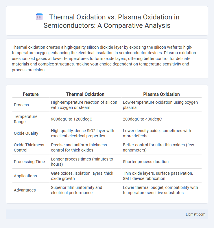
Table of Comparison
| Feature | Thermal Oxidation | Plasma Oxidation |
|---|---|---|
| Process | High-temperature reaction of silicon with oxygen or steam | Low-temperature oxidation using oxygen plasma |
| Temperature Range | 900degC to 1200degC | 200degC to 400degC |
| Oxide Quality | High-quality, dense SiO2 layer with excellent electrical properties | Lower density oxide, sometimes with more defects |
| Oxide Thickness Control | Precise and uniform thickness control for thick oxides | Better control for ultra-thin oxides (few nanometers) |
| Processing Time | Longer process times (minutes to hours) | Shorter process duration |
| Applications | Gate oxides, isolation layers, thick oxide growth | Thin oxide layers, surface passivation, SMT device fabrication |
| Advantages | Superior film uniformity and electrical performance | Lower thermal budget, compatibility with temperature-sensitive substrates |
Introduction to Oxidation Techniques
Thermal oxidation and plasma oxidation are advanced techniques used to grow oxide layers on semiconductor materials, crucial for electronic device fabrication. Thermal oxidation uses high-temperature exposure to oxygen or steam, creating uniform and dense oxide films ideal for integrated circuits. Plasma oxidation operates at lower temperatures by generating reactive oxygen species in a plasma state, enabling precise control over oxide thickness and composition for sensitive substrates.
What is Thermal Oxidation?
Thermal oxidation is a semiconductor fabrication process that grows a silicon dioxide (SiO2) layer on a silicon wafer by exposing it to high-temperature oxygen or steam. This method creates a dense, uniform oxide layer essential for insulating and passivating silicon surfaces in microelectronics. Thermal oxidation offers excellent control over oxide thickness and quality, making it a standard technique for forming gate oxides and isolation layers in integrated circuits.
How Plasma Oxidation Works
Plasma oxidation uses ionized gas containing reactive oxygen species to break down organic contaminants on surfaces at lower temperatures than thermal oxidation. The process involves generating a plasma field through electric discharge, which produces highly reactive radicals that aggressively oxidize pollutants into simpler molecules like CO2 and H2O. This method offers enhanced surface cleaning efficiency with reduced thermal damage, making it suitable for temperature-sensitive materials in semiconductor and environmental applications.
Key Differences Between Thermal and Plasma Oxidation
Thermal oxidation uses high temperatures to grow a silicon dioxide layer by exposing the substrate to oxygen or steam, while plasma oxidation relies on ionized gas to create oxide layers at lower temperatures. Plasma oxidation offers better control over film thickness and uniformity, especially for sensitive materials, compared to the more traditional and higher-temperature thermal oxidation process. Choosing the right method depends on your device requirements for temperature tolerance, oxide quality, and precision.
Process Parameters and Control
Thermal oxidation typically occurs at temperatures between 800degC and 1200degC, with precise control over oxygen flow and ambient conditions to grow uniform silicon dioxide layers. Plasma oxidation operates at significantly lower temperatures, around 300degC to 500degC, utilizing ionized gas species in a plasma state to enhance oxide growth rates while allowing fine-tuned control over plasma power, pressure, and gas composition. Process stability in thermal oxidation is governed by temperature uniformity and gas purity, whereas plasma oxidation demands careful regulation of plasma density and energy to achieve consistent oxide thickness and quality.
Oxide Layer Quality and Properties
Thermal oxidation produces a uniform and dense silicon dioxide layer with excellent electrical insulating properties and low defect density, ideal for high-performance semiconductor devices. Plasma oxidation generates oxide layers at lower temperatures, resulting in thinner films with improved step coverage and enhanced interface quality, beneficial for delicate substrates and advanced microelectronic applications. The choice between these methods depends on the required oxide thickness, interface trap density, and thermal budget constraints in device fabrication.
Applications in Semiconductor Manufacturing
Thermal oxidation and plasma oxidation are critical processes in semiconductor manufacturing for forming high-quality silicon dioxide layers on silicon wafers. Thermal oxidation provides uniform, dense oxide layers essential for gate dielectrics in MOSFETs and isolation structures in integrated circuits. Plasma oxidation enables lower temperature oxide growth, improving compatibility with temperature-sensitive materials and enhancing surface passivation in advanced device fabrication.
Advantages and Limitations of Thermal Oxidation
Thermal oxidation offers high-quality, uniform silicon dioxide layers essential for semiconductor device fabrication with excellent electrical properties and strong interface stability. Its main advantages include scalability, process simplicity, and the ability to produce thick oxide films with low defect densities. Limitations involve high processing temperatures that can induce stress or dopant diffusion, longer cycle times, and substantial energy consumption compared to plasma oxidation methods.
Benefits and Challenges of Plasma Oxidation
Plasma oxidation offers significant benefits including lower processing temperatures, enhanced surface activation, and precise control over oxide layer thickness compared to traditional thermal oxidation. This method reduces thermal stress and is compatible with temperature-sensitive materials, enabling improved performance in semiconductor and thin-film applications. Challenges include the need for specialized equipment, potential plasma-induced damage, and higher initial costs, which may limit widespread adoption despite its advantages.
Choosing the Right Oxidation Method
Choosing the right oxidation method depends on the material properties and desired surface characteristics; thermal oxidation is ideal for uniform, high-quality oxide layers on silicon wafers, while plasma oxidation offers lower temperature processing suitable for delicate substrates. Your semiconductor fabrication process benefits from thermal oxidation's strong oxide reliability, whereas plasma oxidation provides better control over oxide thickness at reduced thermal budgets. Evaluating factors like temperature sensitivity, oxide quality, and process integration ensures optimal selection between thermal and plasma oxidation methods.
Thermal Oxidation vs Plasma Oxidation Infographic