Plasma Ashing offers a dry, chemical-free method for removing photoresist with precise control and minimal substrate damage, making it ideal for delicate semiconductor processes. Wet Ashing uses liquid chemicals to strip residues but may introduce contamination risks and requires proper waste management to ensure safe disposal.
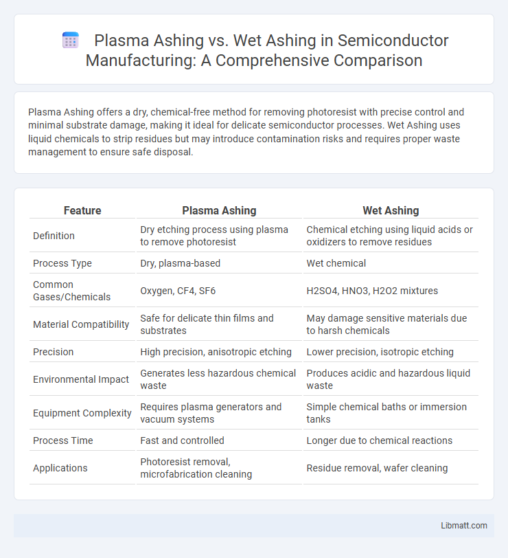
Table of Comparison
| Feature | Plasma Ashing | Wet Ashing |
|---|---|---|
| Definition | Dry etching process using plasma to remove photoresist | Chemical etching using liquid acids or oxidizers to remove residues |
| Process Type | Dry, plasma-based | Wet chemical |
| Common Gases/Chemicals | Oxygen, CF4, SF6 | H2SO4, HNO3, H2O2 mixtures |
| Material Compatibility | Safe for delicate thin films and substrates | May damage sensitive materials due to harsh chemicals |
| Precision | High precision, anisotropic etching | Lower precision, isotropic etching |
| Environmental Impact | Generates less hazardous chemical waste | Produces acidic and hazardous liquid waste |
| Equipment Complexity | Requires plasma generators and vacuum systems | Simple chemical baths or immersion tanks |
| Process Time | Fast and controlled | Longer due to chemical reactions |
| Applications | Photoresist removal, microfabrication cleaning | Residue removal, wafer cleaning |
Introduction to Plasma Ashing and Wet Ashing
Plasma ashing utilizes reactive oxygen plasma to remove organic residues from semiconductor wafers through a dry etching process, offering precise control and reduced chemical waste. Wet ashing involves chemical solutions, typically acids like sulfuric or nitric acid mixed with oxidizers, to oxidize and dissolve organic contaminants from material surfaces. Both techniques are essential in microfabrication and semiconductor industries for effective cleaning but differ in environmental impact, process control, and substrate compatibility.
Principles of Plasma Ashing
Plasma ashing utilizes reactive ionized gases, typically oxygen or fluorine plasma, to remove organic materials by breaking chemical bonds through energetic ion bombardment and chemical reactions. This dry technique creates volatile byproducts that are evacuated, offering precise control over etching depth and minimal substrate damage. In contrast to wet ashing, which relies on liquid chemical solutions for oxidation and removal, plasma ashing operates under low-pressure conditions enabling uniform, anisotropic etching essential for microfabrication processes.
Fundamentals of Wet Ashing
Wet Ashing involves using strong acids or oxidizing agents to chemically digest organic materials, converting them into soluble inorganic forms. This technique is ideal for thorough decomposition of complex matrices in analytical chemistry, ensuring accurate elemental analysis. Your samples benefit from controlled reaction conditions that minimize contamination and preserve analyte integrity.
Key Differences Between Plasma and Wet Ashing
Plasma ashing uses ionized gas to remove organic material with high precision and minimal chemical waste, making it ideal for delicate semiconductor and microelectronics applications. Wet ashing involves strong acids to dissolve contaminants, offering effective bulk material removal but generating hazardous chemical byproducts requiring careful handling. Choosing between plasma and wet ashing depends on Your need for processing speed, environmental safety, and the specific sensitivity of the materials involved.
Advantages of Plasma Ashing
Plasma ashing offers precise and uniform etching with minimal chemical waste, making it an environmentally friendly alternative to traditional wet ashing methods. This dry process enhances control over the removal of organic layers in semiconductor manufacturing, improving yield and reducing contamination risks. You benefit from faster processing times and increased safety due to the absence of harsh liquids and corrosive chemicals.
Benefits of Wet Ashing
Wet ashing offers superior sample digestion by utilizing strong acids to break down complex matrices, ensuring complete mineralization and accurate elemental analysis. Your laboratory benefits from reduced contamination risk and enhanced recovery of trace elements due to the controlled chemical environment. This method is especially advantageous for organic-rich samples and materials requiring thorough oxidation without thermal degradation.
Limitations and Challenges of Each Method
Plasma ashing faces limitations such as reduced effectiveness on high aspect ratio structures and potential damage to sensitive substrates due to ion bombardment. Wet ashing encounters challenges including incomplete removal of certain residues and the use of hazardous chemicals that require careful handling and disposal. Your choice between these methods depends on balancing precision, material compatibility, and environmental safety considerations.
Applications in Industry and Research
Plasma ashing offers precise material removal and is widely used in semiconductor manufacturing for photoresist stripping and cleaning delicate microelectronic surfaces, ensuring high purity. Wet ashing, involving chemical solutions, is preferred in environmental and pharmaceutical analysis for sample digestion due to its efficiency in breaking down organic matrices. Your choice depends on the specific industrial or research application requirements, balancing factors like sample type, contamination risk, and processing speed.
Safety Considerations and Environmental Impact
Plasma ashing offers enhanced safety by eliminating hazardous chemical exposure and reducing toxic waste generation commonly associated with wet ashing, which uses strong acids and produces corrosive effluents. Its low chemical usage and ability to operate at lower temperatures contribute to minimizing environmental impact, making it a cleaner, more sustainable option for sample preparation. Wet ashing requires stringent handling procedures and proper disposal methods to mitigate risks to lab personnel and the environment due to the aggressive reagents involved.
Choosing the Right Ashing Method for Your Needs
Plasma ashing offers precise, dry etching ideal for delicate semiconductor materials, minimizing chemical waste and contamination risks. Wet ashing excels in effectively removing organic residues through strong chemical reactions, beneficial for bulk material cleaning and surface preparation. Selecting the right ashing method depends on substrate sensitivity, desired purity, and environmental considerations, ensuring optimal process control and material compatibility.
Plasma Ashing vs Wet Ashing Infographic