Chip Scale Packaging (CSP) offers a compact, cost-effective solution by packaging individual chips, whereas Wafer Level Chip Scale Packaging (WLCSP) integrates packaging processes directly at the wafer level, enhancing performance and reducing size even further. Your choice between CSP and WLCSP should consider factors like device complexity, production volume, and thermal management requirements.
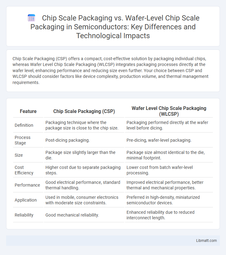
Table of Comparison
| Feature | Chip Scale Packaging (CSP) | Wafer Level Chip Scale Packaging (WLCSP) |
|---|---|---|
| Definition | Packaging technique where the package size is close to the chip size. | Packaging performed directly at the wafer level before dicing. |
| Process Stage | Post-dicing packaging. | Pre-dicing, wafer-level packaging. |
| Size | Package size slightly larger than the die. | Package size almost identical to the die, minimal footprint. |
| Cost Efficiency | Higher cost due to separate packaging steps. | Lower cost from batch wafer-level processing. |
| Performance | Good electrical performance, standard thermal handling. | Improved electrical performance, better thermal and mechanical properties. |
| Application | Used in mobile, consumer electronics with moderate size constraints. | Preferred in high-density, miniaturized semiconductor devices. |
| Reliability | Good mechanical reliability. | Enhanced reliability due to reduced interconnect length. |
Introduction to Chip Scale Packaging (CSP)
Chip Scale Packaging (CSP) reduces the size of semiconductor packages to nearly the same dimensions as the silicon die, enhancing electrical performance and thermal management. CSP offers improved electrical characteristics by minimizing parasitic inductance and capacitance through shorter interconnects, which is crucial for high-speed applications. Your choice of CSP impacts device miniaturization and reliability, making it essential for modern electronics requiring compact, efficient packaging solutions.
What is Wafer Level Chip Scale Packaging (WLCSP)?
Wafer Level Chip Scale Packaging (WLCSP) is an advanced semiconductor packaging technology that enables the entire packaging process to be completed at the wafer level, rather than after individual die are separated. This method enhances performance by reducing package size, improving electrical characteristics, and enabling lower inductance and resistance through direct solder ball connections on the wafer surface. WLCSP is widely used in mobile devices and high-density applications due to its compact form factor and cost-efficiency compared to traditional Chip Scale Packaging (CSP), which packages individual dies post-dicing.
Key Differences Between CSP and WLCSP
Chip Scale Packaging (CSP) typically involves packaging individual semiconductor dies into small packages that are slightly larger than the chip itself, providing improved electrical performance and heat dissipation. Wafer Level Chip Scale Packaging (WLCSP) processes the entire wafer with packaging steps before dicing, resulting in even smaller package sizes and enhanced electrical characteristics due to reduced interconnect length. Key differences include CSP's post-dicing packaging approach versus WLCSP's wafer-level process, with WLCSP offering superior miniaturization and integration for high-performance, space-constrained applications.
Advantages of Chip Scale Packaging
Chip Scale Packaging (CSP) offers significant advantages such as a smaller footprint, which enhances device performance by reducing signal path lengths and improving electrical characteristics. It provides better thermal management and mechanical reliability compared to traditional packaging methods, supporting higher density integration suitable for compact electronic devices. Your designs benefit from CSP's cost-effectiveness and scalability, making it ideal for high-volume production with improved yield and lower overall manufacturing costs.
Benefits of Wafer Level Chip Scale Packaging
Wafer Level Chip Scale Packaging (WLCSP) offers significant advantages over traditional Chip Scale Packaging (CSP) by enabling smaller package size and higher input/output density, which improves device performance and reduces the overall footprint on the PCB. WLCSP processes the entire wafer before dicing, leading to higher throughput, lower manufacturing costs, and enhanced reliability through reduced die handling and improved thermal and electrical characteristics. This packaging technique is especially beneficial for applications demanding miniaturization, such as mobile devices and IoT components, where space efficiency and cost-effectiveness are critical.
Limitations of Traditional CSP
Traditional Chip Scale Packaging (CSP) faces limitations such as larger package sizes and increased parasitic inductance, leading to reduced electrical performance and higher signal loss in high-frequency applications. Thermal management challenges arise due to less efficient heat dissipation compared to Wafer Level Chip Scale Packaging (WLCSP), which offers superior miniaturization by integrating packaging directly at the wafer level. Your designs benefit from WLCSP's finer pitch and improved electrical characteristics, addressing the shortcomings of conventional CSP methods.
Challenges in Wafer Level CSP Implementation
Wafer Level Chip Scale Packaging (WLCSP) faces challenges such as high initial capital investment and intricate process control to ensure die alignment and uniformity across entire wafers. Managing warpage and thermal stress during packaging can impact yield and reliability compared to traditional Chip Scale Packaging (CSP) methods. Advanced inspection and repair techniques are crucial to address defects and maintain production efficiency in WLCSP implementation.
Applications of CSP and WLCSP in Electronics
Chip Scale Packaging (CSP) is widely applied in mobile devices, consumer electronics, and automotive systems due to its compact size and enhanced electrical performance. Wafer Level Chip Scale Packaging (WLCSP) excels in ultra-thin devices like smartphones, wearables, and medical implants, offering superior miniaturization and thermal management. Understanding the differences in your electronics projects can optimize device integration and reliability.
Market Trends: CSP vs. WLCSP
Market trends indicate a growing preference for Wafer Level Chip Scale Packaging (WLCSP) due to its superior miniaturization and cost efficiency compared to traditional Chip Scale Packaging (CSP). WLCSP's direct wafer-level processing enhances electrical performance and reliability, making it ideal for high-demand applications in smartphones, IoT devices, and wearables. Staying informed about these advancements enables Your design strategies to align with industry demands for smaller, more efficient semiconductor components.
Future Outlook for Chip Packaging Technologies
Chip Scale Packaging (CSP) and Wafer Level Chip Scale Packaging (WLCSP) are critical in advancing miniaturization and performance in semiconductor devices. WLCSP offers superior scalability and cost-efficiency by enabling packaging directly at the wafer level, reducing assembly steps and enhancing thermal and electrical performance. Ongoing innovations in materials and process technologies position WLCSP as a leading solution for next-generation high-density, high-speed applications in IoT, 5G, and AI hardware.
Chip Scale Packaging vs Wafer Level Chip Scale Packaging Infographic