Transparent wafers allow light to pass through, making them ideal for optical applications and solar cells, whereas opaque wafers block light and are commonly used in traditional semiconductor devices where light transmission is unnecessary. Choosing the right wafer impacts your device's efficiency and functionality depending on whether light-sensitive performance is required.
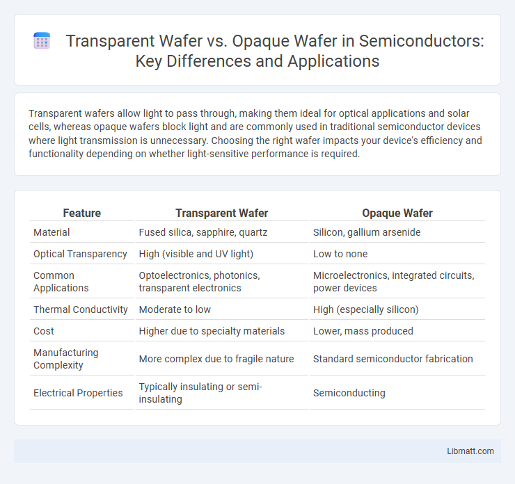
Table of Comparison
| Feature | Transparent Wafer | Opaque Wafer |
|---|---|---|
| Material | Fused silica, sapphire, quartz | Silicon, gallium arsenide |
| Optical Transparency | High (visible and UV light) | Low to none |
| Common Applications | Optoelectronics, photonics, transparent electronics | Microelectronics, integrated circuits, power devices |
| Thermal Conductivity | Moderate to low | High (especially silicon) |
| Cost | Higher due to specialty materials | Lower, mass produced |
| Manufacturing Complexity | More complex due to fragile nature | Standard semiconductor fabrication |
| Electrical Properties | Typically insulating or semi-insulating | Semiconducting |
Introduction to Transparent and Opaque Wafers
Transparent wafers, often made from materials like quartz or sapphire, allow light to pass through them and are essential in optoelectronic applications and photonics. Opaque wafers, usually composed of silicon or other semiconductors, block light transmission and are widely used in integrated circuits and microelectronics manufacturing. Your choice between transparent and opaque wafers depends on the specific requirements of light interaction and electrical performance in your semiconductor devices.
Defining Transparent Wafers
Transparent wafers are semiconductor substrates that allow light to pass through, typically made from materials like sapphire or quartz, unlike opaque wafers composed of silicon or other metals that block light. These transparent wafers enable applications in optoelectronics and photonics by facilitating the integration of light-emitting or light-sensing devices directly on the wafer surface. Your choice between transparent and opaque wafers depends on the specific requirements for light transmission and device functionality in your semiconductor manufacturing process.
Characteristics of Opaque Wafers
Opaque wafers are characterized by their non-transparent properties, typically made from silicon or other crystalline materials, which block light transmission. These wafers possess high mechanical strength, excellent thermal conductivity, and are widely used in traditional semiconductor device fabrication. Their opaque nature makes them suitable for applications requiring robust electrical insulation and light isolation.
Material Composition Differences
Transparent wafers are primarily composed of materials like sapphire or quartz, which have high optical transparency and are suitable for applications requiring light transmission. Opaque wafers, often made from silicon or other semiconductor materials, block light due to their crystalline structure and dopant distribution. Your choice depends on whether optical clarity or electronic properties are prioritized in your device fabrication.
Key Applications of Transparent Wafers
Transparent wafers, commonly made from sapphire or quartz, are essential in optoelectronic devices such as LED substrates, solar cells, and optical sensors due to their excellent light transmission and thermal stability. These wafers enhance efficiency in photonics by enabling precise light manipulation and high-power laser applications. Their unique properties also support advanced display technologies and biomedical imaging systems, where clarity and durability are critical.
Common Uses of Opaque Wafers
Opaque wafers are commonly utilized in solar panel manufacturing, particularly for photovoltaic cells where light absorption and energy conversion efficiency are crucial. They are also widely used in semiconductor devices, including integrated circuits, owing to their stable electrical properties and cost-effectiveness. Their non-transparency makes them ideal for applications requiring strong structural support and protection of underlying layers in electronic components.
Optical Properties Comparison
Transparent wafers exhibit high optical transmittance and lower light absorption, making them ideal for photonic and optoelectronic applications, whereas opaque wafers primarily reflect or absorb light, limiting their use in these fields. The refractive index of transparent wafers enables precise light manipulation and minimal scattering, while opaque wafers typically cause higher optical losses. Material composition, such as silicon dioxide for transparent wafers and crystalline silicon for opaque wafers, directly influences their optical behavior and suitability for various semiconductor applications.
Manufacturing Process Variations
Transparent wafers, typically made from materials like sapphire or quartz, require specialized fabrication processes involving high-temperature crystal growth and precision polishing to maintain optical clarity, contrasting with the conventional silicon-based opaque wafers produced through the Czochralski or Float Zone methods. The manufacturing of transparent wafers demands stringent control of impurities and defects to ensure transparency and optical performance, whereas opaque wafers focus more on electrical purity and crystalline uniformity. Process variations in doping, temperature control, and surface treatment distinctly influence the final wafer properties due to the differing physical and chemical characteristics of transparent versus opaque semiconductor substrates.
Advantages and Limitations of Each Type
Transparent wafers offer superior optical properties, enabling efficient light transmission crucial for photonic and optoelectronic devices, but they often face challenges in mechanical strength and heat dissipation. Opaque wafers provide robust structural integrity and better thermal management, making them suitable for high-power semiconductor applications, yet their limited light transmission restricts use in optical technologies. Selecting between transparent and opaque wafers depends on the specific requirements for optical clarity versus durability and thermal performance in semiconductor device fabrication.
Future Trends in Wafer Technology
Future trends in wafer technology emphasize transparent wafers, which offer enhanced optical properties for advanced photonic and optoelectronic applications, surpassing traditional opaque silicon wafers. Innovations in materials like sapphire and silicon carbide enable higher efficiency and integration in sensors, solar cells, and flexible electronics. Your choice between transparent and opaque wafers will increasingly depend on requirements for light transmission and device performance in next-generation semiconductor designs.
Transparent Wafer vs Opaque Wafer Infographic