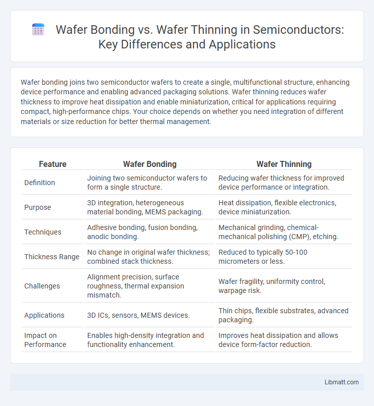
Wafer bonding joins two semiconductor wafers to create a single, multifunctional structure, enhancing device performance and enabling advanced packaging solutions. Wafer thinning reduces wafer thickness to improve heat dissipation and enable miniaturization, critical for applications requiring compact, high-performance chips. Your choice depends on whether you need integration of different materials or size reduction for better thermal management.
Table of Comparison
| Feature | Wafer Bonding | Wafer Thinning |
|---|---|---|
| Definition | Joining two semiconductor wafers to form a single structure. | Reducing wafer thickness for improved device performance or integration. |
| Purpose | 3D integration, heterogeneous material bonding, MEMS packaging. | Heat dissipation, flexible electronics, device miniaturization. |
| Techniques | Adhesive bonding, fusion bonding, anodic bonding. | Mechanical grinding, chemical-mechanical polishing (CMP), etching. |
| Thickness Range | No change in original wafer thickness; combined stack thickness. | Reduced to typically 50-100 micrometers or less. |
| Challenges | Alignment precision, surface roughness, thermal expansion mismatch. | Wafer fragility, uniformity control, warpage risk. |
| Applications | 3D ICs, sensors, MEMS devices. | Thin chips, flexible substrates, advanced packaging. |
| Impact on Performance | Enables high-density integration and functionality enhancement. | Improves heat dissipation and allows device form-factor reduction. |
Introduction to Wafer Bonding and Wafer Thinning
Wafer bonding is a crucial semiconductor process that involves joining two or more wafers to create a single, integrated unit with improved structural integrity and electrical performance. Wafer thinning, on the other hand, refers to reducing the wafer thickness to enhance heat dissipation and enable advanced packaging solutions. Understanding these techniques allows you to optimize device fabrication for better efficiency and reliability in microelectronics.
Fundamental Concepts: Wafer Bonding Explained
Wafer bonding is a critical semiconductor process where two or more wafers are permanently joined to create a single, integrated structure with enhanced functionality and performance. This technique involves aligning and bonding wafers using methods like direct bonding, anodic bonding, or adhesive bonding, enabling high-quality electrical and mechanical connections. Understanding wafer bonding fundamentals helps optimize your semiconductor device fabrication by improving wafer integration and achieving superior device reliability.
Fundamental Concepts: Wafer Thinning Explained
Wafer thinning is a critical semiconductor fabrication process that reduces the thickness of a silicon wafer to enhance device performance, thermal management, and integration density. Unlike wafer bonding, which joins two wafers to create a composite structure, wafer thinning involves mechanical grinding, chemical etching, or plasma processes to achieve precise thickness control. Your semiconductor devices benefit from wafer thinning by enabling advanced packaging techniques and improving electrical characteristics through minimized bulk material.
Key Differences Between Wafer Bonding and Wafer Thinning
Wafer bonding involves joining two semiconductor wafers to create a single, unified structure, enhancing device functionality and integration. Wafer thinning, on the other hand, reduces the thickness of a wafer to improve thermal management and mechanical flexibility in semiconductor devices. The key differences lie in their objectives: wafer bonding focuses on combining wafers, while wafer thinning aims to reduce wafer thickness for performance optimization.
Materials and Techniques Used in Wafer Bonding
Wafer bonding involves joining two semiconductor wafers using techniques such as direct bonding, anodic bonding, or adhesive bonding, relying on materials like silicon, glass, and polymers to achieve strong, hermetic seals. The process often uses surface activation methods, including plasma treatment and chemical-mechanical polishing, to enhance interface adhesion and reduce void formation. Your device performance benefits from precise control over bonding parameters and careful material selection to ensure mechanical stability and electrical integrity.
Processes and Methods of Wafer Thinning
Wafer thinning primarily involves mechanical grinding, chemical mechanical polishing (CMP), and plasma etching to reduce wafer thickness for improved device performance and integration. Mechanical grinding quickly removes bulk material, while CMP achieves ultra-smooth surfaces critical for subsequent processing steps. Plasma etching offers precise thickness control with minimal damage, complementing traditional thinning methods in semiconductor manufacturing.
Advantages and Challenges of Wafer Bonding
Wafer bonding offers significant advantages, including the ability to integrate heterogeneous materials, enabling enhanced device performance and functionality in applications such as 3D integrated circuits and MEMS devices. Challenges include achieving defect-free interfaces, managing thermal expansion mismatches, and ensuring strong adhesion while maintaining wafer surface quality. Despite these challenges, wafer bonding remains critical for advanced semiconductor manufacturing processes that require high-density integration and miniaturization.
Benefits and Limitations of Wafer Thinning
Wafer thinning offers significant benefits including enhanced electrical performance, improved thermal management, and reduced package size, which are crucial for advanced semiconductor devices. However, limitations such as increased fragility, higher risk of die warpage, and complex handling requirements can impact yield and manufacturing costs. Understanding these trade-offs helps you optimize wafer-level processes for high-performance and miniaturized electronic applications.
Applications: When to Use Wafer Bonding vs Wafer Thinning
Wafer bonding is ideal for applications requiring the integration of heterogeneous materials, such as 3D integrated circuits, MEMS devices, and sensor packaging, where combining multiple wafers enhances functionality and performance. Wafer thinning is preferred in applications demanding ultra-thin wafers for improved heat dissipation, flexible electronics, and advanced semiconductor devices that require reduced substrate thickness for enhanced electrical characteristics. Choosing between wafer bonding and wafer thinning depends on whether the goal is to structurally integrate multiple wafers or to reduce wafer thickness for mechanical and electrical optimization.
Future Trends in Wafer Bonding and Thinning Technologies
Emerging wafer bonding techniques emphasize improved alignment accuracy and material compatibility to support advanced 3D integration and heterogeneous device architectures, while future wafer thinning methods focus on achieving ultra-thin, defect-free layers with enhanced mechanical stability for flexible electronics and high-performance sensors. Innovations in plasma-assisted bonding and atomic layer etching contribute to higher precision and scalability in wafer-level packaging and MEMS device fabrication. Integration of AI-driven process control is expected to optimize both wafer bonding and thinning processes, reducing costs and enhancing yield in semiconductor manufacturing.
Wafer Bonding vs Wafer Thinning Infographic