LVTTL (Low Voltage TTL) and LVCMOS (Low Voltage CMOS) are two common digital logic signal standards primarily used in integrated circuits, with LVTTL operating at 3.3V and featuring TTL input thresholds while LVCMOS supports various lower voltage levels like 1.8V and offers lower power consumption and faster switching speeds. Your choice depends on compatibility with other components and power efficiency needs, as LVCMOS is generally preferred for modern, low-power applications.
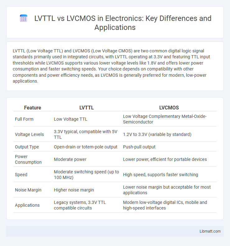
Table of Comparison
| Feature | LVTTL | LVCMOS |
|---|---|---|
| Full Form | Low Voltage TTL | Low Voltage Complementary Metal-Oxide-Semiconductor |
| Voltage Levels | 3.3V typical, compatible with 5V TTL | 1.2V to 3.3V (variable by standard) |
| Output Type | Open-drain or totem-pole output | Push-pull output |
| Power Consumption | Moderate power | Lower power, efficient for portable devices |
| Speed | Moderate switching speed (up to 100 MHz) | High speed, supports faster switching |
| Noise Margin | Higher noise margin | Lower noise margin but acceptable for most applications |
| Applications | Legacy systems, 3.3V TTL compatible circuits | Modern low-voltage digital ICs, mobile and high-speed interfaces |
Introduction to LVTTL and LVCMOS Logic Standards
LVTTL (Low Voltage Transistor-Transistor Logic) and LVCMOS (Low Voltage Complementary Metal-Oxide-Semiconductor) are fundamental digital logic standards used for interfacing integrated circuits. LVTTL operates with a voltage range typically around 3.3V and features faster switching speeds but higher power consumption, while LVCMOS supports a wider voltage range from 1.2V to 3.3V, offering lower power consumption and improved noise margins. Understanding the differences in voltage thresholds and drive strengths between LVTTL and LVCMOS is crucial for optimizing your circuit design and ensuring signal compatibility.
Definition and Technical Specifications of LVTTL
LVTTL (Low Voltage Transistor-Transistor Logic) operates at a lower voltage level compared to standard TTL, typically utilizing a 3.3V power supply. It achieves faster switching speeds and reduced power consumption, with input voltage thresholds generally around 0.8V for low and 2.0V for high logic levels. LVTTL is commonly used in digital integrated circuits where compatibility with 3.3V logic systems and improved noise margins are critical.
Definition and Technical Specifications of LVCMOS
LVCMOS (Low Voltage Complementary Metal-Oxide-Semiconductor) is a popular logic signaling standard defined by operating voltages typically ranging from 1.2V to 3.3V, optimizing low power consumption and high-speed data transfer. It provides improved noise immunity and stricter voltage thresholds compared to LVTTL (Low Voltage Transistor-Transistor Logic), making it suitable for modern high-density digital circuits. Your choice between LVTTL and LVCMOS depends on voltage compatibility and signal integrity requirements in the design environment.
Key Differences Between LVTTL and LVCMOS
LVTTL (Low-Voltage Transistor-Transistor Logic) operates typically at 3.3V with defined threshold voltages for input and output levels, making it suitable for TTL-compatible systems. LVCMOS (Low-Voltage Complementary Metal-Oxide-Semiconductor) supports a wider voltage range from 1.2V to 3.3V and offers lower power consumption with CMOS-compatible input thresholds. The primary differences lie in voltage levels, power efficiency, switching speed, and noise margins, where LVCMOS generally provides better power efficiency and flexibility in voltage supply compared to LVTTL.
Voltage Levels and Electrical Characteristics
LVTTL (Low Voltage TTL) operates with a typical voltage level of 3.3V, featuring input thresholds around 0.8V (low) and 2.0V (high), while LVCMOS (Low Voltage CMOS) supports a wider range of supply voltages from 1.2V to 3.3V, offering higher noise margins and lower power consumption. Electrical characteristics of LVTTL include higher input current and faster rise/fall times, whereas LVCMOS provides lower input leakage currents and reduced power dissipation, making it more suitable for modern low-voltage digital circuits. Your choice between LVTTL and LVCMOS should consider the specific voltage compatibility and power efficiency requirements of your application.
Power Consumption Comparison
LVTLL generally consumes less power than LVCMOS, especially at lower voltages due to its lower switching threshold and reduced static current. LVCMOS, while popular for its noise immunity, tends to draw higher dynamic power during switching because of its higher voltage swings. This makes LVTTL a preferred choice for power-sensitive applications aiming to minimize overall energy consumption in digital circuits.
Signal Integrity and Noise Margin
LVTTL offers a smaller noise margin compared to LVCMOS, typically around 0.4V versus 1.2V, making LVCMOS more robust in noisy environments. Signal integrity in LVCMOS is generally better due to its lower voltage swings and reduced susceptibility to crosstalk and electromagnetic interference. When choosing between LVTTL and LVCMOS, consider that your design will benefit from LVCMOS if higher noise immunity and cleaner signal transmission are critical factors.
Compatibility and Interfacing Considerations
LVTTL (Low-Voltage TTL) and LVCMOS (Low-Voltage CMOS) logic families differ in voltage levels and input/output characteristics, affecting their compatibility and interfacing. LVTTL typically operates at 3.3V with input thresholds around 0.8V to 2V, while LVCMOS supports a wider voltage range (1.8V to 3.3V) and has input thresholds closer to half the supply voltage, making direct interfacing sometimes problematic without level shifting. Designers must carefully assess signal voltage levels, drive strengths, and noise margins to ensure reliable communication between LVTTL and LVCMOS devices in mixed-logic systems.
Applications of LVTTL vs LVCMOS
LVTTL (Low Voltage TTL) is predominantly used in applications requiring compatibility with legacy TTL logic levels, such as older microcontrollers, FPGA interfaces, and communication protocols where 3.3V signal levels are essential. LVCMOS (Low Voltage CMOS) excels in modern digital circuits demanding lower power consumption and higher noise margins, making it ideal for high-speed microprocessors, memory modules, and advanced integrated circuits operating at voltages as low as 1.8V. The choice between LVTTL and LVCMOS hinges on the device's voltage requirements, power efficiency considerations, and interface compatibility within embedded systems and consumer electronics.
Choosing the Right Logic Standard for Your Design
LVTTL and LVCMOS are popular logic standards with distinct voltage levels and noise margins, influencing their suitability for different circuit designs. LVTTL operates typically at 3.3V with TTL-compatible input thresholds, making it ideal for interfacing with legacy TTL devices, while LVCMOS supports a wider range of supply voltages from 1.2V to 3.3V, offering lower power consumption and faster switching speeds. Selecting the right logic standard depends on design requirements such as voltage compatibility, power efficiency, and signal integrity within mixed-signal systems.
LVTTL vs LVCMOS Infographic