Plated Through Holes (PTH) traverse the entire printed circuit board thickness, providing reliable connections between all layers, while Blind Vias connect only the outer layers to one or more inner layers, enhancing signal integrity and saving space on high-density PCBs. Choosing the right via type depends on your board's complexity, electrical requirements, and manufacturing budget.
Table of Comparison
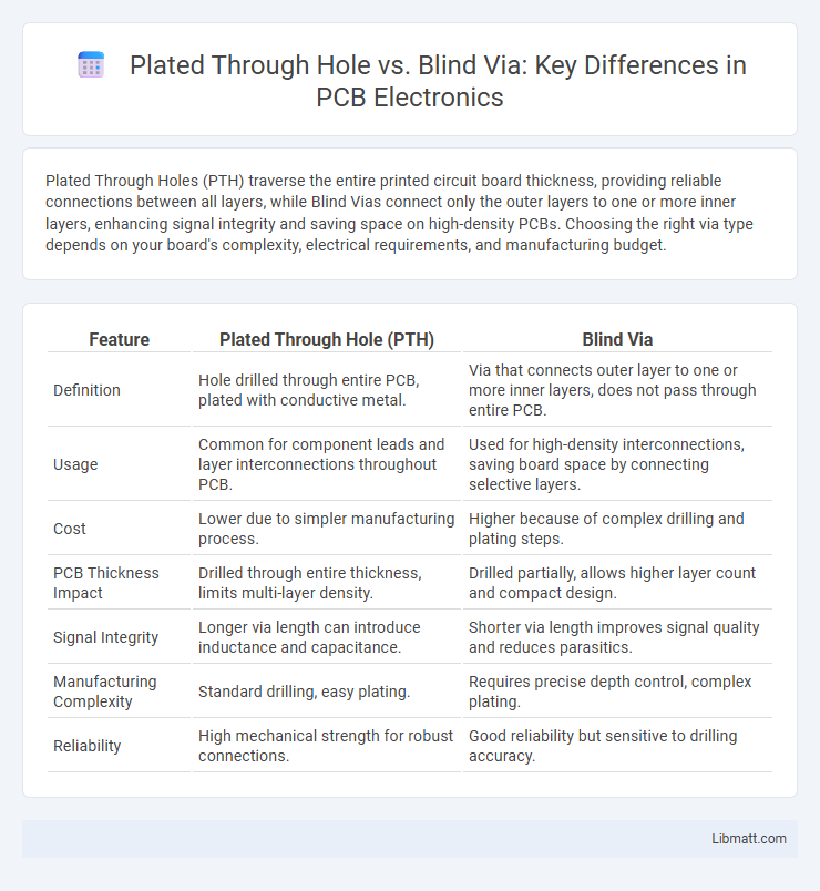
| Feature | Plated Through Hole (PTH) | Blind Via |
|---|---|---|
| Definition | Hole drilled through entire PCB, plated with conductive metal. | Via that connects outer layer to one or more inner layers, does not pass through entire PCB. |
| Usage | Common for component leads and layer interconnections throughout PCB. | Used for high-density interconnections, saving board space by connecting selective layers. |
| Cost | Lower due to simpler manufacturing process. | Higher because of complex drilling and plating steps. |
| PCB Thickness Impact | Drilled through entire thickness, limits multi-layer density. | Drilled partially, allows higher layer count and compact design. |
| Signal Integrity | Longer via length can introduce inductance and capacitance. | Shorter via length improves signal quality and reduces parasitics. |
| Manufacturing Complexity | Standard drilling, easy plating. | Requires precise depth control, complex plating. |
| Reliability | High mechanical strength for robust connections. | Good reliability but sensitive to drilling accuracy. |
Overview of Plated Through Hole and Blind Via
Plated Through Hole (PTH) is a PCB technology where a conductive hole passes entirely through the board, enabling reliable electrical connections between all layers. Blind Via, on the other hand, connects outer layers to one or more inner layers without going through the entire board, optimizing space and signal performance. Your PCB design choice depends on factors like layer count, board thickness, and signal integrity requirements.
Key Differences Between PTH and Blind Via
Plated Through Holes (PTH) are conductive holes that extend through the entire PCB thickness, enabling electrical connections between all layers, whereas Blind Vias connect only the outer layer to one or more inner layers without passing through the entire board. PTHs offer mechanical robustness and reliable electrical continuity but consume more board space, while Blind Vias save surface area and improve signal integrity in high-density designs by limiting the via depth. Manufacturing complexity and cost are higher for Blind Vias due to precise drilling and plating processes compared to the more straightforward production of PTHs.
Manufacturing Process Comparison
Plated Through Hole (PTH) vias are manufactured by drilling holes completely through the PCB layers, followed by plating the hole walls with copper to create electrical connections. Blind vias are formed by drilling partially through the PCB layers and plating only the hole walls that connect outer layers to inner layers, avoiding full penetration. The manufacturing process of blind vias is more complex, requiring precise depth control and advanced drilling equipment compared to the straightforward drilling method used for PTH vias.
Electrical Performance Considerations
Plated Through Holes (PTHs) typically offer lower electrical resistance and inductance due to their full-depth copper plating, enabling reliable signal transmission across multiple PCB layers. Blind vias, which connect only select layers, reduce parasitic capacitance and crosstalk, enhancing high-frequency signal integrity in dense multilayer designs. Choosing between PTH and blind via depends on balancing electrical performance requirements with board complexity and layer count in high-speed applications.
Mechanical Strength and Reliability
Plated Through Holes (PTH) provide superior mechanical strength due to their continuous metal plating throughout the entire PCB thickness, ensuring robust structural support and reliable electrical connections. Blind Vias, which only connect outer layers to one or more inner layers without passing through the entire board, offer limited mechanical strength and may be more prone to stress-related failures under thermal cycling or mechanical strain. For applications demanding high reliability and durability, especially in harsh environments, PTHs are typically preferred over blind vias.
Space-Saving and Design Flexibility
Plated Through Hole (PTH) and Blind Via technologies differ significantly in space-saving and design flexibility within PCB layouts. Blind vias connect only outer layers to internal layers, reducing board real estate usage and enabling higher component density, while PTHs pass through the entire board, consuming more space and limiting routing options. Your choice between PTH and blind vias impacts overall PCB compactness and the complexity of multilayer circuit designs.
Cost Implications: PTH vs Blind Via
Plated Through Hole (PTH) technology generally incurs higher costs due to increased material usage and more complex drilling processes compared to Blind Vias, which only penetrate partially through the PCB layers. Blind Vias require advanced laser drilling techniques, raising fabrication expenses but enable higher density circuit designs, potentially reducing overall board size and materials costs. Cost implications depend on design complexity and volume, with PTH favored for simpler, lower-layer count PCBs and Blind Vias preferred in high-density interconnects where space-saving justifies higher manufacturing costs.
Common Applications in PCB Design
Plated Through Holes (PTH) are widely used in PCB design for mounting through-hole components and providing robust mechanical support and electrical connectivity across all layers, ideal for connectors and large components. Blind Vias connect outer layers to one or more inner layers without penetrating the entire board, making them suitable for high-density interconnect (HDI) designs where space conservation is critical, such as in smartphones and compact electronics. Both PTHs and Blind Vias enhance multilayer PCB functionality but target different application needs based on board complexity and component placement.
Limitations and Challenges of Each Technology
Plated Through Hole (PTH) technology faces limitations in high-density designs due to increased board size and signal integrity issues caused by longer via lengths. Blind Vias challenge manufacturing complexity and cost because of restricted drill depths and the need for precise layer alignment, which can result in higher defect rates. Both technologies require careful consideration of thermal management, mechanical stress, and electrical performance to optimize reliability in multilayer PCB fabrication.
Choosing the Right Via for Your PCB Project
Choosing the right via for your PCB project involves understanding the differences between plated through holes (PTH) and blind vias. PTHs provide reliable electrical connections through the entire board thickness and are ideal for designs requiring strong mechanical support and easy inspection. Blind vias connect outer layers to one or more inner layers without passing through the entire board, saving space and improving signal integrity in high-density, multi-layer PCBs, which is crucial for optimizing your circuit performance.
Plated Through Hole vs Blind Via Infographic