Chemical Vapor Deposition (CVD) uses chemical reactions to deposit thin films on substrates, offering precise control over film composition and uniformity, while Physical Vapor Deposition (PVD) relies on physical processes like evaporation or sputtering to coat surfaces, typically achieving higher purity but with less conformality. Your choice depends on specific application requirements such as coating complexity, substrate temperature tolerance, and desired film properties.
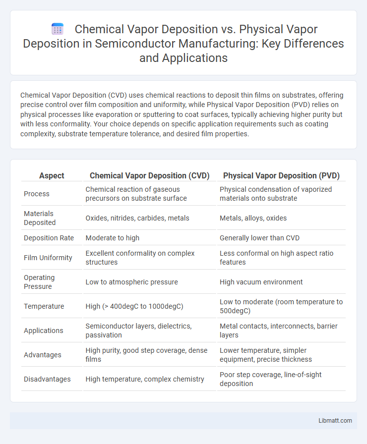
Table of Comparison
| Aspect | Chemical Vapor Deposition (CVD) | Physical Vapor Deposition (PVD) |
|---|---|---|
| Process | Chemical reaction of gaseous precursors on substrate surface | Physical condensation of vaporized materials onto substrate |
| Materials Deposited | Oxides, nitrides, carbides, metals | Metals, alloys, oxides |
| Deposition Rate | Moderate to high | Generally lower than CVD |
| Film Uniformity | Excellent conformality on complex structures | Less conformal on high aspect ratio features |
| Operating Pressure | Low to atmospheric pressure | High vacuum environment |
| Temperature | High (> 400degC to 1000degC) | Low to moderate (room temperature to 500degC) |
| Applications | Semiconductor layers, dielectrics, passivation | Metal contacts, interconnects, barrier layers |
| Advantages | High purity, good step coverage, dense films | Lower temperature, simpler equipment, precise thickness |
| Disadvantages | High temperature, complex chemistry | Poor step coverage, line-of-sight deposition |
Introduction to Vapor Deposition Techniques
Chemical Vapor Deposition (CVD) and Physical Vapor Deposition (PVD) are critical vapor deposition techniques used to create thin films and coatings in semiconductor manufacturing and materials science. CVD involves chemical reactions of gaseous precursors on a substrate surface to form a solid material, often resulting in highly conformal and uniform coatings. In contrast, PVD relies on physical processes such as sputtering or evaporation to deposit material, offering precise control over film thickness and composition without chemical reactions.
What is Chemical Vapor Deposition (CVD)?
Chemical Vapor Deposition (CVD) is a process used to produce high-quality, high-performance solid materials by depositing a thin film from a vapor phase chemical reaction onto a substrate. Unlike Physical Vapor Deposition (PVD), which relies on physical processes like sputtering or evaporation, CVD involves chemical reactions that form a solid material directly on your target surface, often resulting in superior conformity and coverage. This technique is widely utilized in semiconductor manufacturing, coating aerospace components, and producing protective layers on medical devices.
What is Physical Vapor Deposition (PVD)?
Physical Vapor Deposition (PVD) is a vacuum-based coating technique that involves the physical transfer of material from a source to a substrate, forming thin films for enhanced surface properties. Common PVD methods include sputtering and evaporation, used extensively in semiconductor manufacturing, optics, and tool coating due to their ability to produce high-purity, uniform layers. PVD offers advantages such as lower processing temperatures and superior adhesion compared to Chemical Vapor Deposition (CVD), making it ideal for temperature-sensitive materials.
Key Differences Between CVD and PVD
Chemical Vapor Deposition (CVD) and Physical Vapor Deposition (PVD) differ primarily in their deposition mechanisms, with CVD relying on chemical reactions to produce thin films and PVD using physical processes such as sputtering or evaporation. CVD typically achieves better conformality on complex surfaces and higher film quality, while PVD offers more precise control over film thickness and composition. Your choice depends on factors like substrate temperature tolerance, desired film properties, and coating uniformity requirements.
Materials Suitable for CVD vs PVD
Chemical Vapor Deposition (CVD) is ideal for depositing high-purity, high-performance materials such as silicon carbide, tungsten, and diamond-like carbon, making it suitable for semiconductor and hard coating applications. Physical Vapor Deposition (PVD) excels with metals like aluminum, titanium, and chromium, offering excellent adhesion and uniform thin films for decorative and wear-resistant coatings. Understanding the material compatibility of CVD and PVD helps optimize Your manufacturing process for superior film quality and application-specific performance.
Process Steps: CVD vs PVD
Chemical Vapor Deposition (CVD) involves chemical reactions of vapor-phase precursors on a heated substrate, forming a solid material layer through decomposition or chemical reaction. Physical Vapor Deposition (PVD) deposits thin films by physical processes such as evaporation or sputtering, where atoms are ejected from a target material and condense onto the substrate surface. Your choice between CVD and PVD depends on the required film properties, as CVD offers conformal coatings with strong adhesion, while PVD provides high-purity, dense films with precise thickness control.
Applications of CVD in Industry
Chemical Vapor Deposition (CVD) finds extensive applications in the semiconductor industry for fabricating high-purity, high-performance thin films used in microelectronics, photovoltaic cells, and MEMS devices. It is also crucial in the production of protective coatings in aerospace and automotive industries, enhancing wear resistance and corrosion protection. Your production processes benefit from CVD's ability to uniformly coat complex geometries, which Physical Vapor Deposition (PVD) techniques may struggle to achieve.
Applications of PVD in Industry
Physical Vapor Deposition (PVD) is widely used in industries for coating tools, automotive parts, and electronic components due to its ability to produce hard, wear-resistant, and corrosion-resistant surfaces. PVD is essential in semiconductor manufacturing for thin-film deposition and is also prevalent in decorative finishes for watches and jewelry. You can enhance product durability and performance by leveraging PVD's precision and versatility in various industrial applications.
Advantages and Limitations of CVD and PVD
Chemical Vapor Deposition (CVD) offers advantages such as superior film conformity, excellent step coverage, and the ability to coat complex geometries with high purity and density. Physical Vapor Deposition (PVD) provides high deposition rates, precise thickness control, and lower processing temperatures, making it suitable for temperature-sensitive substrates. Your choice between CVD and PVD depends on factors like substrate compatibility, film properties required, and process complexity, as CVD may involve higher temperatures and more intricate equipment, while PVD can be limited in coating uniformity on complex shapes.
Choosing the Right Deposition Method for Your Needs
Chemical Vapor Deposition (CVD) offers superior conformality and film uniformity, making it ideal for complex geometries and high-volume semiconductor manufacturing. Physical Vapor Deposition (PVD) provides excellent control over film thickness and is preferred for materials sensitive to high temperatures, commonly used in decorative coatings and thin film applications. Evaluating your specific requirements such as substrate compatibility, desired film properties, and production scale ensures you select the optimal deposition method for your project.
Chemical Vapor Deposition vs Physical Vapor Deposition Infographic