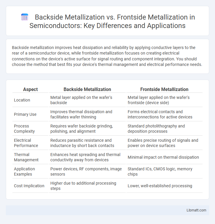
Backside metallization improves heat dissipation and reliability by applying conductive layers to the rear of a semiconductor device, while frontside metallization focuses on creating electrical connections on the device's active surface for signal routing and component integration. You should choose the method that best fits your device's thermal management and electrical performance needs.
Table of Comparison
| Aspect | Backside Metallization | Frontside Metallization |
|---|---|---|
| Location | Metal layer applied on the wafer's backside | Metal layer applied on the wafer's frontside (device side) |
| Primary Use | Improves thermal dissipation and facilitates wafer thinning | Forms electrical contacts and interconnections for active devices |
| Process Complexity | Requires wafer backside grinding, polishing, and alignment | Standard photolithography and deposition processes |
| Electrical Performance | Reduces parasitic resistance and inductance by short back contacts | Enables precise routing of signals and power on device surfaces |
| Thermal Management | Enhances heat spreading and thermal conductivity away from devices | Minimal impact on thermal dissipation |
| Application Examples | Power devices, RF components, image sensors | Standard ICs, CMOS logic, memory chips |
| Cost Implication | Higher due to additional processing steps | Lower, well-established processing |
Introduction to Metallization in Semiconductor Devices
Metallization in semiconductor devices involves depositing metal layers to form electrical contacts and interconnections, essential for device functionality. Backside metallization refers to metal layers applied on the wafer's rear side, improving heat dissipation and electrical performance in power devices, while frontside metallization covers active device areas for signal routing and bonding. Your choice between backside and frontside metallization impacts device reliability, electrical resistance, and manufacturing complexity in semiconductor fabrication.
Overview of Backside Metallization
Backside metallization involves applying metal layers to the rear side of semiconductor wafers to enhance electrical conductivity and improve heat dissipation. This technique is critical for creating reliable backside contacts in high-power devices and advanced solar cells, enabling better performance and device longevity. Compared to frontside metallization, which focuses on the wafer's active side, backside metallization offers unique advantages in reducing shading and increasing active surface area utilization.
Overview of Frontside Metallization
Frontside metallization involves applying metal contacts and interconnections on the device's active surface, crucial for efficient current collection and transparent electrode formation. This process optimizes light absorption by minimizing shading losses on solar cells, enhancing overall device efficiency. Your choice of frontside metallization techniques directly impacts electrical performance and cost-effectiveness in semiconductor manufacturing.
Key Differences between Backside and Frontside Metallization
Backside metallization involves applying conductive layers on the rear surface of a semiconductor wafer, enhancing heat dissipation and enabling better electrical contact for high-power devices. Frontside metallization is performed on the wafer's top surface, primarily for interconnecting active components and ensuring signal routing in integrated circuits. Key differences include their functional roles, with backside metallization improving thermal management and mechanical support, while frontside metallization focuses on circuit connectivity and device performance integration.
Materials Used in Backside vs Frontside Metallization
Backside metallization primarily uses silver or aluminum-silver alloys to enhance electrical conductivity and improve solderability on the rear side of solar cells, while frontside metallization typically employs silver paste for finer grid lines to maximize light absorption and minimize shading. The silver in frontside metallization must be highly conductive yet capable of forming thin, precise patterns, whereas backside metallization materials are optimized for mechanical robustness and efficient current collection without obstructing cell illumination. Your choice of metallization materials directly influences cell efficiency, durability, and manufacturing cost.
Process Steps for Backside Metallization
Backside metallization involves applying metal contacts on the rear side of a semiconductor wafer, enhancing device performance by improving heat dissipation and electrical connectivity. Key process steps include wafer cleaning, deposition of a barrier layer to prevent diffusion, followed by metal layer sputtering or evaporation, and subsequent annealing to ensure strong adhesion and electrical conductivity. You benefit from reduced shading on the frontside, maximizing light absorption and overall efficiency in photovoltaic and microelectronic applications.
Process Steps for Frontside Metallization
Frontside metallization involves precise deposition of metal contacts on the photoactive surface of a solar cell, starting with surface cleaning, followed by applying a thin metal seed layer through sputtering or evaporation. Photolithography defines specific patterns, after which electroplating or screen printing adds thicker metal layers for enhanced conductivity. The process concludes with annealing to improve adhesion and electrical performance, ensuring optimal charge collection and cell efficiency.
Advantages and Disadvantages of Backside Metallization
Backside metallization offers significant advantages such as improved thermal management, enhanced mechanical stability, and increased photovoltaic cell efficiency by minimizing shading losses on the front side. However, this approach faces challenges including complex processing steps, higher manufacturing costs, and potential issues with metal adhesion and uniformity on the wafer's rear surface. Your choice between backside and frontside metallization should consider these trade-offs in efficiency gains versus production complexity.
Advantages and Disadvantages of Frontside Metallization
Frontside metallization offers improved electrical contact and reduced resistance due to direct exposure to sunlight, enhancing solar cell efficiency and current collection. However, it can cause shading losses as metal lines obstruct light absorption, negatively impacting overall energy output. Your choice depends on balancing enhanced conductivity with the trade-off of decreased active cell area.
Applications and Future Trends in Metallization Technologies
Backside metallization is predominantly used in solar cell applications to enhance electrical contact and improve overall efficiency by minimizing shading on the front surface, while frontside metallization remains vital for establishing conductive pathways and enabling effective light absorption. Emerging trends emphasize advanced materials like silver nanowires and conductive polymers for frontside metallization, whereas backside methods are evolving towards passivated contacts and innovative plating techniques to reduce resistive losses. Your choice between these metallization technologies should consider the application-specific requirements and anticipated advancements, such as perovskite solar cells integration and flexible electronics, which are shaping the future landscape of metallization technologies.
Backside Metallization vs Frontside Metallization Infographic