Wafer cleaning removes contaminants and particles from the wafer surface to ensure optimal device performance, while wafer etching selectively removes material to create intricate patterns and structures. Your choice depends on whether you need surface purification or precise material removal for semiconductor fabrication.
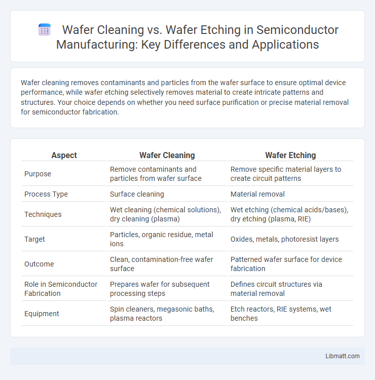
Table of Comparison
| Aspect | Wafer Cleaning | Wafer Etching |
|---|---|---|
| Purpose | Remove contaminants and particles from wafer surface | Remove specific material layers to create circuit patterns |
| Process Type | Surface cleaning | Material removal |
| Techniques | Wet cleaning (chemical solutions), dry cleaning (plasma) | Wet etching (chemical acids/bases), dry etching (plasma, RIE) |
| Target | Particles, organic residue, metal ions | Oxides, metals, photoresist layers |
| Outcome | Clean, contamination-free wafer surface | Patterned wafer surface for device fabrication |
| Role in Semiconductor Fabrication | Prepares wafer for subsequent processing steps | Defines circuit structures via material removal |
| Equipment | Spin cleaners, megasonic baths, plasma reactors | Etch reactors, RIE systems, wet benches |
Introduction to Wafer Cleaning and Wafer Etching
Wafer cleaning involves the removal of contaminants such as particles, organic residues, and metal ions from semiconductor wafers to ensure surface purity and improve device performance. Wafer etching is a microfabrication process that selectively removes material from the wafer surface using chemical or plasma techniques to create patterns for integrated circuits. Both processes are critical in semiconductor manufacturing, with cleaning ensuring defect-free surfaces and etching enabling precise pattern transfer.
Importance of Surface Preparation in Semiconductor Manufacturing
Surface preparation in semiconductor manufacturing is critical for ensuring wafer cleanliness and defect-free layering. Wafer cleaning removes contaminants such as particles, organic residues, and metals that can impair device performance, while wafer etching precisely modifies surface topology to create circuit patterns and improve adhesion. Effective surface preparation enhances device yield, reliability, and electrical characteristics in microelectronics fabrication processes.
Wafer Cleaning: Processes and Techniques
Wafer cleaning involves removing contaminants such as particles, organic residues, and metal ions from semiconductor wafers using processes like RCA cleaning, solvent cleaning, and megasonic cleaning to ensure surface purity and enhance device performance. Techniques such as wet chemical cleaning with solutions like SC-1 (ammonium hydroxide, hydrogen peroxide) and SC-2 (hydrochloric acid, hydrogen peroxide) target specific contaminants without damaging the wafer. Advanced cleaning methods include plasma cleaning and ultraviolet ozone cleaning, which improve surface energy for better thin-film adhesion in semiconductor fabrication.
Types of Contaminants Targeted by Wafer Cleaning
Wafer cleaning targets organic residues, metallic particles, and native oxides that can compromise semiconductor device performance, ensuring the removal of particles as small as a few nanometers. Unlike wafer etching, which selectively removes material layers to shape patterns, cleaning focuses on eliminating contaminants without altering the wafer's substrate. Your semiconductor manufacturing process benefits from precise wafer cleaning techniques to maintain surface integrity and enhance yield.
Wafer Etching: Methods and Applications
Wafer etching involves precise removal of material from semiconductor wafers using methods such as wet chemical etching, reactive ion etching (RIE), and plasma etching, each offering varying degrees of anisotropy and selectivity essential for microfabrication. Applications of wafer etching include pattern transfer in photolithography, creation of high-aspect-ratio structures, and surface texturing for improved device performance in integrated circuits and MEMS devices. The choice of etching method directly impacts device yield, feature resolution, and overall semiconductor manufacturing quality.
Differences Between Wet Etching and Dry Etching
Wet etching utilizes liquid chemicals to selectively remove material from the wafer surface, offering precise control over undercutting but limited by isotropic etch profiles. Dry etching employs plasma or reactive gases, enabling anisotropic etching with high directional control, vital for advanced semiconductor device fabrication. The choice between wet and dry etching depends on factors like desired etch profile, material selectivity, and integration with subsequent process steps in wafer manufacturing.
Comparative Analysis: Cleaning vs Etching
Wafer cleaning focuses on the removal of organic, inorganic, and particulate contaminants from the wafer surface using chemical solutions or ultrasonic methods, ensuring high surface purity without material loss. Wafer etching involves the selective removal of wafer material through chemical or plasma processes to define circuit patterns, which directly alters surface topology and feature dimensions. Cleaning preserves the wafer's integrity for subsequent processing, whereas etching precisely shapes the wafer at micro and nanoscale levels essential for semiconductor device fabrication.
Factors Influencing the Choice: Cleaning or Etching
The choice between wafer cleaning and wafer etching is influenced primarily by the type and extent of contamination, as well as the desired surface modification. Cleaning is favored for removing organic residues, particles, and native oxides without altering the wafer's topography, while etching is selected to selectively remove material layers or modify surface morphology with chemical or plasma processes. Process parameters such as chemical selectivity, etch rate, surface sensitivity, and compatibility with subsequent fabrication steps dictate whether cleaning or etching is the optimal approach.
Challenges and Solutions in Wafer Cleaning and Etching
Wafer cleaning faces challenges such as particle contamination and chemical residues that can degrade device performance, while solutions include using advanced megasonic agitation and optimized chemical formulations to enhance contaminant removal. Wafer etching challenges include achieving precise pattern transfer and minimizing surface damage, addressed through techniques like reactive ion etching (RIE) and atomic layer etching (ALE) for improved control and selectivity. Integration of real-time process monitoring and end-point detection systems further mitigates defects in both cleaning and etching stages, ensuring higher yield and device reliability.
Future Trends in Wafer Cleaning and Etching Technologies
Future trends in wafer cleaning and etching technologies emphasize advanced nano-scale precision and environmentally sustainable processes to meet the demands of next-generation semiconductor manufacturing. Innovations in plasma etching and megasonic cleaning leverage artificial intelligence and real-time monitoring to enhance accuracy, reduce defects, and increase throughput. Your semiconductor fabrication can benefit from these cutting-edge solutions that optimize surface treatment while minimizing chemical waste and energy consumption.
Wafer Cleaning vs Wafer Etching Infographic