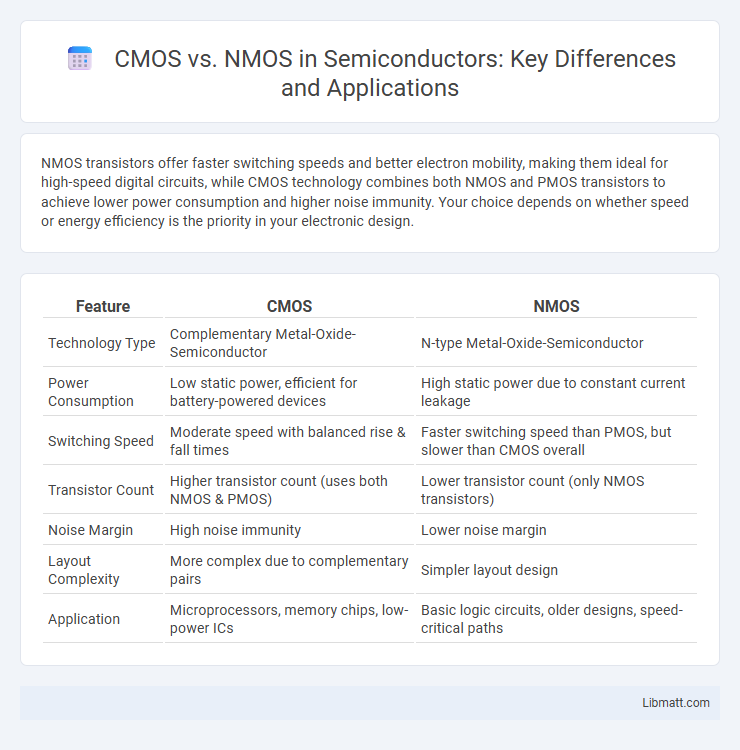
NMOS transistors offer faster switching speeds and better electron mobility, making them ideal for high-speed digital circuits, while CMOS technology combines both NMOS and PMOS transistors to achieve lower power consumption and higher noise immunity. Your choice depends on whether speed or energy efficiency is the priority in your electronic design.
Table of Comparison
| Feature | CMOS | NMOS |
|---|---|---|
| Technology Type | Complementary Metal-Oxide-Semiconductor | N-type Metal-Oxide-Semiconductor |
| Power Consumption | Low static power, efficient for battery-powered devices | High static power due to constant current leakage |
| Switching Speed | Moderate speed with balanced rise & fall times | Faster switching speed than PMOS, but slower than CMOS overall |
| Transistor Count | Higher transistor count (uses both NMOS & PMOS) | Lower transistor count (only NMOS transistors) |
| Noise Margin | High noise immunity | Lower noise margin |
| Layout Complexity | More complex due to complementary pairs | Simpler layout design |
| Application | Microprocessors, memory chips, low-power ICs | Basic logic circuits, older designs, speed-critical paths |
Introduction to CMOS and NMOS Technologies
CMOS (Complementary Metal-Oxide-Semiconductor) and NMOS (N-type Metal-Oxide-Semiconductor) are fundamental semiconductor technologies used in integrated circuit design. CMOS technology leverages both NMOS and PMOS transistors to achieve low power consumption and high noise immunity, making it ideal for modern digital devices. NMOS technology, which utilizes only n-type transistors, offers faster switching speeds but typically consumes more power, influencing your choice based on performance and energy efficiency requirements.
Basic Structure of CMOS and NMOS
CMOS (Complementary Metal-Oxide-Semiconductor) consists of both p-type and n-type MOSFETs arranged in a complementary manner to achieve low power consumption, while NMOS (N-type Metal-Oxide-Semiconductor) uses only n-type MOSFETs. The basic CMOS structure includes parallel pMOS transistors connected to the positive supply voltage and series nMOS transistors connected to ground, enabling efficient switching and minimal static power dissipation. In contrast, NMOS circuits rely solely on nMOS transistors typically configured with pull-up resistors or loads, resulting in higher static power consumption and reduced noise margins compared to CMOS designs.
Operating Principles: CMOS vs NMOS
CMOS technology uses complementary pairs of p-type and n-type MOSFETs, where p-channel devices conduct when the input is low and n-channel devices conduct when the input is high, ensuring low power consumption during switching. NMOS circuits rely solely on n-type MOSFETs, which conduct when a positive voltage is applied to the gate, but require a pull-up resistor or transistor for proper logic operation, resulting in higher static power dissipation. CMOS's complementary operation enables efficient digital logic with minimal power use, while NMOS's simpler structure offers faster switching speeds but at the cost of increased power consumption.
Power Consumption Comparison
CMOS technology significantly reduces power consumption compared to NMOS by utilizing both PMOS and NMOS transistors, which only draw current during switching events, minimizing static power dissipation. NMOS circuits continuously consume power when in the 'on' state due to a direct path between the supply voltage and ground, leading to higher static power loss. Your choice of CMOS over NMOS enables more energy-efficient designs, especially critical in battery-powered and portable devices.
Speed and Performance Differences
NMOS transistors exhibit faster switching speeds due to higher electron mobility compared to CMOS, which combines both NMOS and PMOS devices for balanced performance and power efficiency. CMOS technology reduces static power consumption significantly but may have slightly lower speed than pure NMOS circuits in high-frequency applications. When optimizing Your design for speed, consider NMOS for critical paths while using CMOS to achieve overall power-performance trade-offs.
Fabrication Process Overview
CMOS (Complementary Metal-Oxide-Semiconductor) integrates both NMOS (N-type Metal-Oxide-Semiconductor) and PMOS transistors on the same substrate, requiring additional fabrication steps such as dual doping processes, precise photolithographic masking, and separate well formations for p-type and n-type regions. NMOS fabrication is simpler with only n-type transistor processing, involving fewer implantation steps and a single well type, which can lead to faster manufacturing and lower cost but higher static power consumption. Understanding the distinct fabrication complexities helps optimize Your semiconductor design choices for power efficiency and integration density.
Advantages of CMOS Over NMOS
CMOS technology offers significantly lower power consumption than NMOS due to its complementary transistor arrangement, which reduces static power dissipation. It provides better noise immunity and higher density integration, enabling more complex and efficient circuits. CMOS also supports both n-type and p-type transistors, allowing for faster switching speeds and improved overall performance in digital applications.
Limitations of NMOS Technology
NMOS technology faces limitations such as higher static power consumption due to its inability to completely turn off current flow, leading to increased leakage currents. The absence of complementary p-type transistors results in lower noise margins and reduced switching speed compared to CMOS technology. Furthermore, NMOS circuits suffer from higher power dissipation and reduced device scalability, impacting overall energy efficiency and integration density in modern microelectronics.
Applications in Modern Electronics
CMOS technology dominates modern electronics due to its low power consumption and high noise immunity, making it ideal for integrated circuits in microprocessors, memory chips, and digital logic circuits. NMOS transistors, while faster in switching speed, are primarily used in specific analog applications, RF circuits, and certain high-speed digital circuits where power efficiency is less critical. The widespread adoption of CMOS in smartphones, laptops, and IoT devices highlights its superiority in balancing performance and energy efficiency for contemporary electronic applications.
Future Trends in Semiconductor Devices
Future trends in semiconductor devices highlight the increasing adoption of CMOS technology due to its superior energy efficiency and scalability compared to NMOS. Advanced CMOS processes enable smaller transistor sizes, reduced power consumption, and enhanced performance, making them ideal for next-generation applications like AI and IoT. Emerging materials and 3D integration techniques further accelerate CMOS innovation, surpassing traditional NMOS limitations in speed and density.
CMOS vs NMOS Infographic