Silicon photonics offers cost-effective, high-volume integration with mature CMOS technology, making it ideal for data centers and telecommunications. III-V photonics provides superior performance in light emission and amplification, essential for laser sources and high-speed optical communication, enhancing your photonic system's efficiency and functionality.
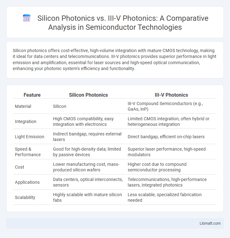
Table of Comparison
| Feature | Silicon Photonics | III-V Photonics |
|---|---|---|
| Material | Silicon | III-V Compound Semiconductors (e.g., GaAs, InP) |
| Integration | High CMOS compatibility, easy integration with electronics | Limited CMOS integration, often hybrid or heterogeneous integration |
| Light Emission | Indirect bandgap, requires external lasers | Direct bandgap, efficient on-chip lasers |
| Speed & Performance | Good for high-density data; limited by passive devices | Superior laser performance, high-speed modulators |
| Cost | Lower manufacturing cost, mass-produced silicon wafers | Higher cost due to compound semiconductor processing |
| Applications | Data centers, optical interconnects, sensors | Telecommunications, high-performance lasers, integrated photonics |
| Scalability | Highly scalable with mature silicon fabs | Less scalable, specialized fabrication needed |
Introduction to Silicon Photonics and III-V Photonics
Silicon photonics utilizes silicon as the primary material for optical components, enabling high-density integration with existing CMOS technology and facilitating cost-effective, scalable photonic circuits. III-V photonics leverages compound semiconductors like gallium arsenide or indium phosphide, offering superior optical gain and high-efficiency light emission essential for lasers and advanced optoelectronic devices. These complementary technologies drive innovation in data communications, optical interconnects, and photonic integrated circuits by balancing integration potential and optical performance.
Core Material Platforms: Silicon vs III-V Semiconductors
Silicon photonics utilizes silicon as the core material platform, benefiting from its compatibility with CMOS technology and mature fabrication processes, which enable cost-effective mass production and integration with electronic circuits. III-V semiconductors, such as gallium arsenide (GaAs) and indium phosphide (InP), offer superior optoelectronic properties including direct bandgap for efficient light emission and detection, making them ideal for high-performance lasers and photodetectors. The fundamental distinction lies in silicon's indirect bandgap limiting active light generation, whereas III-V materials excel in active photonic components but face higher fabrication complexity and costs.
Photonic Device Integration Capabilities
Silicon photonics excels in photonic device integration by leveraging mature CMOS fabrication processes, enabling high-density integration of photonic components with electronic circuits on a single chip. III-V photonics offers superior material properties for active devices like lasers and modulators, but integrating these materials with silicon substrates typically requires complex heterogeneous integration techniques. Your choice depends on whether you prioritize large-scale integration and cost-efficiency (silicon photonics) or advanced optoelectronic functionalities with high performance (III-V photonics).
Performance Metrics: Speed, Loss, and Bandwidth
Silicon photonics offers high bandwidth and integration density with moderate optical loss but often faces speed limitations due to silicon's indirect bandgap. III-V photonics, utilizing materials like indium phosphide, delivers superior speed and lower optical loss, enabling faster modulation and improved signal integrity. Your choice hinges on balancing silicon photonics' cost-effectiveness and integration with III-V's enhanced speed and bandwidth performance metrics.
Manufacturing Scalability and Cost Comparison
Silicon photonics benefits from mature CMOS manufacturing processes, enabling high-volume production with lower costs and excellent scalability for large-scale integration. III-V photonics, while offering superior optical performance and direct light emission, typically involves more complex and expensive fabrication steps, limiting cost efficiency and scalability compared to silicon-based approaches. Your choice depends on balancing cost-effectiveness and manufacturability against specific optical performance requirements.
Applications in Data Centers and Telecommunications
Silicon Photonics offers cost-effective, high-bandwidth solutions ideal for data center interconnects due to its compatibility with CMOS manufacturing, enabling large-scale integration and low power consumption. III-V Photonics provides superior performance in telecommunications through efficient light emission and direct integration of lasers, supporting long-haul and high-speed optical communication. Your choice depends on whether scalability and cost or optical performance and wavelength versatility are prioritized for your data center or telecom network requirements.
Challenges in Light Source Integration
Silicon photonics faces significant challenges in light source integration due to silicon's indirect bandgap, which limits efficient on-chip laser emission, necessitating hybrid approaches like bonding III-V materials. III-V photonics naturally excels in light source performance with direct bandgap semiconductors, but integrating these materials onto silicon substrates introduces complexity, cost, and yield issues. Overcoming thermal mismatch and lattice dislocations remains critical for reliable and scalable III-V on silicon light sources in advanced photonic systems.
Power Consumption and Thermal Management
Silicon photonics typically offers lower power consumption due to its compatibility with CMOS technology, enabling efficient integration of electronic and photonic components on a single chip. III-V photonics, while providing superior performance in terms of light emission and wavelength range, generally requires more power and complex thermal management systems because of higher heat generation from active materials like indium phosphide or gallium arsenide. Effective thermal management in III-V devices often involves advanced cooling techniques to maintain performance and reliability, unlike silicon photonics which benefits from better thermal conductivity of the silicon substrate.
Future Trends and Research Directions
Silicon photonics is advancing with integration of CMOS-compatible processes, enabling scalable, cost-effective optical interconnects for data centers and high-performance computing, while research targets improving modulators and detectors to overcome silicon's indirect bandgap limitations. III-V photonics continues to excel in high-efficiency light emission and detection, with future trends focused on heterogeneous integration and monolithic growth on silicon substrates to combine its superior optoelectronic properties with silicon's scalability. Emerging directions emphasize hybrid photonic integration and novel materials like quantum dots and 2D materials to enhance performance, energy efficiency, and functionality in telecom, sensing, and quantum information technologies.
Conclusion: Choosing the Right Photonic Platform
Selecting the optimal photonic platform depends on application requirements such as integration density, performance, and cost. Silicon photonics excels in CMOS compatibility and scalability for data communication, while III-V photonics offers superior optoelectronic properties for high-efficiency lasers and photodetectors. Balancing silicon's low-cost mass production with III-V's high-performance components enables tailored hybrid solutions suited for advanced photonic integrated circuits.
Silicon Photonics vs III-V Photonics Infographic