KGD (Known Good Die) ensures your semiconductor components have been fully tested and verified before packaging, significantly reducing failures in final products. Standard Die may not undergo the same rigorous testing, potentially increasing the risk of defects during assembly or operation.
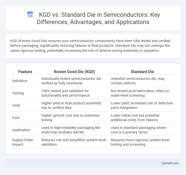
Table of Comparison
| Feature | Known Good Die (KGD) | Standard Die |
|---|---|---|
| Definition | Individually tested semiconductor die verified as fully functional | Untested semiconductor die, may contain defects |
| Testing | 100% tested and validated for functionality and performance | Not tested post-fabrication, relies on wafer-level screening |
| Yield | Higher yield in final product assembly due to verified dies | Lower yield; increased risk of defective parts integration |
| Cost | Higher upfront cost due to extensive testing | Lower initial cost but potential additional costs from failures |
| Application | Used in high-reliability packaging like multi-chip modules (MCM) | Used in standard packaging where cost is a primary factor |
| Supply Chain Impact | Reduces risk and simplifies system-level validation | Requires more rigorous system-level testing and screening |
Introduction to KGD vs Standard Die
KGD (Known Good Die) refers to semiconductor dies that have been individually tested and verified for functionality before packaging, ensuring higher reliability and yield in electronic assemblies. Standard die are untested chips directly sourced from wafer fabrication, posing a risk of integrating defective components into your products. Choosing KGD over standard die significantly reduces failure rates and improves overall system performance in critical applications.
Key Definitions: KGD and Standard Die
Known Good Die (KGD) refers to semiconductor dies that have passed thorough electrical testing and inspection, ensuring high reliability and functionality before packaging or assembly. Standard Dies are raw semiconductor wafers that have not undergone such rigorous testing, potentially containing defects or performance variability. The distinction between KGD and Standard Die is critical for applications requiring high yield and quality assurance in microelectronics manufacturing.
Manufacturing Processes Compared
KGD (Known Good Die) manufacturing involves thorough pre-assembly testing to identify functional semiconductor dies, ensuring only defect-free units proceed to packaging, which reduces waste and improves yield. Standard die production often includes bulk wafer-level testing but may allow untested or partially tested dies into the assembly phase, increasing the risk of packaging faulty units. The KGD process requires advanced probe testing and sorting technologies, enhancing overall product reliability and minimizing downstream failures compared to standard die manufacturing processes.
Quality Control and Testing Methods
KGD (Known Good Die) undergoes rigorous quality control and advanced testing methods, including wafer-level electrical tests and detailed failure analysis, ensuring defect-free components before packaging. Standard die typically experiences less stringent testing, which may increase the risk of latent defects affecting device reliability. Your projects benefit from KGD's enhanced quality assurance, reducing rework and improving overall yield rates.
Performance and Reliability Differences
KGD (Known Good Die) offers superior performance by ensuring each die is tested and verified before assembly, reducing the risk of faulty chips impacting your device's functionality. Standard Die lacks this rigorous pre-testing, often resulting in lower yield and potentially higher failure rates during operation. Choosing KGD can significantly enhance overall reliability and long-term device stability in advanced semiconductor applications.
Cost Implications: KGD vs Standard Die
Known Good Die (KGD) offer higher upfront costs due to rigorous testing and validation processes compared to Standard Die, which are less expensive initially but carry higher risks of latent defects. The use of KGD reduces downstream manufacturing failures and improves yield rates, ultimately lowering total cost of ownership in high-reliability applications. Standard Die may be cost-effective for low-volume or less critical products where the risk of defects has a minimal financial impact.
Applications and Industry Use Cases
KGD (Known Good Die) and Standard Die are pivotal in semiconductor manufacturing, with KGD being critical for high-reliability applications such as aerospace, medical devices, and automotive electronics where tested, defect-free dies ensure system integrity. Standard Die suits cost-sensitive consumer electronics and large-scale production environments where full die-level testing is less critical. Industries demanding stringent quality and performance, like aerospace and automotive, heavily rely on KGD to minimize failure rates and enhance product reliability.
Supply Chain and Availability
KGD (Known Good Die) offers significant supply chain advantages over standard die by reducing the risk of defective components during assembly, leading to higher yield rates and lower rework costs. Standard die availability can be limited by testing failures and variations, causing delays and unpredictability in manufacturing schedules. Utilizing KGD streamlines procurement processes and improves inventory reliability, ensuring consistent production flow and reduced lead times.
Challenges and Limitations
KGD (Known Good Die) faces significant challenges in ensuring high yield due to stringent testing requirements and potential damage during wafer dicing and handling. Standard Die struggles with variability and lower reliability because of less rigorous screening, increasing the risk of faulty components in final assemblies. Both methods encounter limitations related to test cost, throughput, and the complexity of integrating dies into multi-chip modules or advanced packaging solutions.
Future Trends in Die Technology
KGD (Known Good Die) technology is set to transform semiconductor manufacturing by significantly reducing failure rates and improving yield through rigorous pre-assembly testing, outpacing Standard Die approaches. Emerging trends emphasize integrating AI-driven diagnostics and real-time data analytics to enhance KGD accuracy, enabling faster identification of defects and optimizing supply chain efficiency. The shift toward heterogeneous integration and 3D packaging further necessitates reliable KGD processes to ensure high-performance, miniaturized electronic systems in future advanced applications.
KGD vs Standard Die Infographic