Dual Damascene technology enhances semiconductor fabrication by integrating both trench and via formation in a single process, improving circuit density and performance compared to Single Damascene, which creates trenches and vias separately. Your chip designs benefit from Dual Damascene's efficiency and reduced manufacturing complexity, enabling finer interconnects and lower parasitic capacitance.
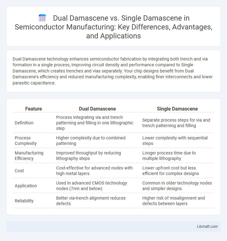
Table of Comparison
| Feature | Dual Damascene | Single Damascene |
|---|---|---|
| Definition | Process integrating via and trench patterning and filling in one lithographic step | Separate process steps for via and trench patterning and filling |
| Process Complexity | Higher complexity due to combined patterning | Lower complexity with sequential steps |
| Manufacturing Efficiency | Improved throughput by reducing lithography steps | Longer process time due to multiple lithography |
| Cost | Cost-effective for advanced nodes with high metal layers | Lower upfront cost but less efficient for complex designs |
| Application | Used in advanced CMOS technology nodes (7nm and below) | Common in older technology nodes and simpler designs |
| Reliability | Better via-trench alignment reduces defects | Higher risk of misalignment and defects between layers |
Introduction to Damascene Processes
The Damascene process in semiconductor fabrication involves creating intricate copper interconnects by etching trenches and vias into an insulating layer, followed by copper deposition and chemical-mechanical polishing. Single Damascene focuses on either the via or trench patterning in one step, while Dual Damascene integrates the formation of both vias and trenches in a single process, improving efficiency and alignment accuracy. Dual Damascene is widely adopted for advanced nodes due to its ability to reduce processing steps and enhance copper interconnect reliability in complex integrated circuits.
Understanding Dual Damascene
Dual Damascene process involves etching both the trench and via patterns in dielectric layers before simultaneous copper deposition, enhancing electrical performance and reducing fabrication steps. Single Damascene fabricates either trenches or vias separately, often requiring multiple metallization steps, which can increase manufacturing complexity and cost. Understanding Dual Damascene allows you to appreciate its advantages in producing fine-pitch interconnects with improved reliability and scalability in advanced semiconductor devices.
Overview of Single Damascene
Single Damascene is a semiconductor fabrication process used to create individual metal interconnect layers by patterning trenches and filling them with metal, typically copper or aluminum. This method simplifies processing by focusing on one metal layer at a time, making it suitable for less complex integrated circuits and reducing defect risks during manufacturing. Your design choice depends on balancing the single layer's ease against the multi-layer efficiency offered by more advanced techniques like Dual Damascene.
Process Steps Comparison
Dual Damascene involves a two-step etching process where trenches and vias are patterned sequentially in dielectric layers before copper metallization, improving alignment accuracy and reducing manufacturing complexity. Single Damascene requires separate patterning and etching steps for trenches and vias, often leading to additional processing time and higher risks of misalignment. Your choice between the two impacts process efficiency, with Dual Damascene typically offering streamlined steps and enhanced integration for advanced semiconductor devices.
Material Utilization Differences
Dual Damascene processes utilize copper more efficiently by integrating trench and via patterning into a single step, reducing the need for multiple deposition and etching cycles. Single Damascene involves separate patterning steps for trenches and vias, often leading to increased material waste due to additional masking and etching. The integrated nature of dual damascene minimizes copper over-plating and enhances overall material economy in semiconductor interconnect fabrication.
Advantages of Dual Damascene
Dual Damascene offers significant advantages over Single Damascene in semiconductor manufacturing by enabling simultaneous formation of interconnect vias and metal lines, which reduces process steps and improves alignment accuracy. This approach enhances circuit density and performance by allowing finer feature control and minimizing parasitic resistance and capacitance. Consequently, Dual Damascene supports advanced technology nodes with higher throughput and better reliability in integrated circuits.
Benefits of Single Damascene
Single Damascene technology simplifies the fabrication process by using a single patterning step to create interconnects, reducing manufacturing complexity and costs. This approach enhances yield reliability by minimizing alignment issues common in Dual Damascene methods, which require two separate patterning steps for vias and trenches. Your semiconductor production benefits from faster turnaround times and improved process control with Single Damascene integration.
Key Applications in Semiconductor Manufacturing
Dual damascene is predominantly utilized in advanced copper interconnect fabrication for integrated circuits, enabling simultaneous patterning of trenches and vias to reduce processing steps and improve alignment accuracy. Single damascene, commonly used in earlier CMOS technologies, focuses on creating either trenches or vias individually, suitable for simpler interconnect layers with aluminum wiring. High-performance microprocessors and memory devices leverage dual damascene for enhanced copper interconnect density and reliability, while single damascene remains relevant in cost-sensitive applications requiring fewer metallization layers.
Challenges and Limitations
Dual Damascene faces challenges such as increased process complexity and alignment accuracy due to multiple lithography and etching steps required for interconnect formation. Single Damascene is limited by the inability to integrate via and trench etching in one step, resulting in lower interconnect density and throughput. Your semiconductor manufacturing efficiency depends on balancing these limitations with specific device design and performance requirements.
Future Trends in Damascene Technology
Future trends in Damascene technology emphasize enhanced patterning precision and reduced manufacturing complexity, with Dual Damascene processes gaining traction due to their ability to simultaneously define metal lines and vias, improving circuit density and performance. Single Damascene techniques remain relevant for simpler wiring schemes but may face limitations as device scaling continues toward sub-5nm nodes, driving innovation toward multi-patterning and advanced materials integration. Your semiconductor manufacturing strategy should consider Dual Damascene advancements to future-proof device reliability and cost-effectiveness in next-generation IC fabrication.
Dual Damascene vs Single Damascene Infographic