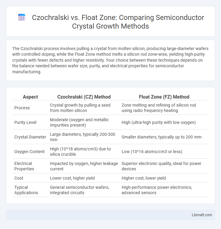
The Czochralski process involves pulling a crystal from molten silicon, producing large-diameter wafers with controlled doping, while the Float Zone method melts a silicon rod zone-wise, yielding high-purity crystals with fewer defects and higher resistivity. Your choice between these techniques depends on the balance needed between wafer size, purity, and electrical properties for semiconductor manufacturing.
Table of Comparison
| Aspect | Czochralski (CZ) Method | Float Zone (FZ) Method |
|---|---|---|
| Process | Crystal growth by pulling a seed from molten silicon | Zone melting and refining of silicon rod using radio frequency heating |
| Purity Level | Moderate (oxygen and metallic impurities present) | High (ultra-high purity with low oxygen) |
| Crystal Diameter | Large diameters, typically 200-300 mm | Smaller diameters, typically up to 200 mm |
| Oxygen Content | High (10^18 atoms/cm3) due to silica crucible | Low (10^16 atoms/cm3 or less) |
| Electrical Properties | Impacted by oxygen, higher leakage current | Superior electronic quality, ideal for power devices |
| Cost | Lower cost, higher yield | Higher cost, lower yield |
| Typical Applications | General semiconductor wafers, integrated circuits | High-performance power electronics, advanced sensors |
Introduction to Silicon Crystal Growth Methods
Czochralski and Float Zone are two primary methods for producing high-purity silicon crystals essential in semiconductor manufacturing. The Czochralski process involves drawing a single crystal from molten silicon using a seed crystal, offering high throughput but with oxygen incorporation. Float Zone, on the other hand, refines silicon through localized melting and solidification without crucible contact, yielding ultra-pure crystals with minimal impurities, ideal for high-performance electronic devices. Understanding these techniques helps optimize Your semiconductor materials for specific industry applications.
Overview of the Czochralski Process
The Czochralski process involves pulling a single crystal ingot from molten semiconductor material, typically silicon, to produce high-purity monocrystalline wafers. This method allows precise control of crystal diameter and doping levels, making it ideal for large-scale semiconductor manufacturing. Compared to Float Zone, Czochralski is more common due to its scalability and lower equipment complexity despite slightly higher oxygen incorporation.
Float Zone Method Explained
The Float Zone method involves melting a narrow region of a silicon crystal using radio frequency induction heating while slowly moving it along the rod, creating highly pure, defect-free semiconductor material. This technique produces silicon with fewer oxygen impurities compared to the Czochralski method, making it ideal for high-performance power devices and detectors. Float Zone silicon exhibits superior electrical properties due to its reduced oxygen and carbon content, enhancing device reliability and efficiency.
Purity Comparison: Czochralski vs Float Zone
Float Zone silicon boasts higher purity levels than Czochralski silicon due to its crucible-free process, which minimizes contamination from container materials. The Czochralski method involves melting silicon in a quartz crucible, introducing oxygen impurities typically around 10^18 atoms/cm3, while Float Zone silicon contains oxygen concentrations as low as 10^16 atoms/cm3. Your semiconductor applications benefit from Float Zone silicon's superior purity, crucial for high-performance electronic devices requiring minimal defects.
Crystal Quality and Defect Levels
Czochralski (CZ) silicon crystals often exhibit higher oxygen content and associated defects due to the contact with the crucible, which can impact electrical properties, whereas Float Zone (FZ) silicon crystals have superior purity and significantly lower oxygen and carbon levels, resulting in fewer crystal defects and enhanced electronic performance. The FZ method produces crystals with minimal dislocations and enhanced uniformity, making them ideal for high-power and high-frequency semiconductor devices. Your choice between CZ and FZ silicon should consider the required crystal quality and defect tolerances for optimal device efficiency and reliability.
Cost and Scalability Considerations
Czochralski (CZ) method offers lower initial costs and higher throughput, making it more scalable for large-volume silicon wafer production compared to the Float Zone (FZ) method. Float Zone technique delivers superior silicon purity and fewer defects, but its higher operational expenses and smaller wafer sizes limit scalability for mass manufacturing. Your choice depends on balancing cost-efficiency against the need for ultra-high purity and performance in semiconductor applications.
Applications in Semiconductor Manufacturing
Czochralski (CZ) crystals are widely used for producing large-diameter silicon wafers essential in mainstream semiconductor manufacturing due to their scalability and cost-effectiveness. Float Zone (FZ) crystals provide ultra-high purity and low oxygen content, making them ideal for high-performance power devices and advanced integrated circuits requiring superior electronic properties. Your choice between CZ and FZ methods depends on the balance between wafer size, purity requirements, and specific semiconductor application needs.
Electrical Properties: Conductivity and Resistivity
Czochralski silicon typically exhibits lower resistivity and higher conductivity due to oxygen impurities incorporated during the crystal pulling process, which can influence carrier concentration. Float Zone silicon offers superior electrical properties with higher resistivity and lower intrinsic doping, making it ideal for high-power and high-frequency semiconductor applications. Your choice between these methods should consider the balance between conductivity and resistivity requirements for optimal device performance.
Environmental and Energy Impacts
The Czochralski method consumes more energy due to its reliance on high-temperature melting in crucibles, leading to greater environmental emissions compared to the Float Zone technique. Float Zone processing, which uses localized heating and avoids crucibles, results in lower impurity levels and reduced energy consumption, making it more environmentally sustainable. Selecting Float Zone silicon can enhance the eco-efficiency of your semiconductor manufacturing by minimizing energy usage and waste generation.
Future Trends in Silicon Wafer Production
Future trends in silicon wafer production emphasize advanced Czochralski and Float Zone methods to meet increasing demands for high-purity, defect-free substrates essential for semiconductor applications. Innovations in Czochralski growth focus on improving crystal uniformity and reducing oxygen contamination, while Float Zone techniques evolve to enable larger diameter wafers with ultra-low impurity levels. Your choice of wafer production can impact device performance and manufacturing scalability as these methods adapt to emerging technologies in microelectronics and photovoltaics.
Czochralski vs Float Zone Infographic