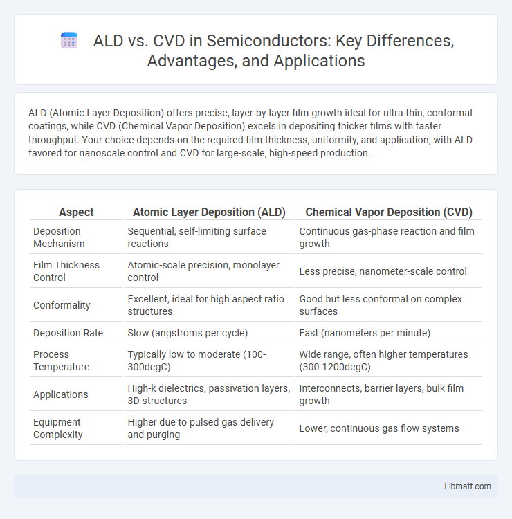
ALD (Atomic Layer Deposition) offers precise, layer-by-layer film growth ideal for ultra-thin, conformal coatings, while CVD (Chemical Vapor Deposition) excels in depositing thicker films with faster throughput. Your choice depends on the required film thickness, uniformity, and application, with ALD favored for nanoscale control and CVD for large-scale, high-speed production.
Table of Comparison
| Aspect | Atomic Layer Deposition (ALD) | Chemical Vapor Deposition (CVD) |
|---|---|---|
| Deposition Mechanism | Sequential, self-limiting surface reactions | Continuous gas-phase reaction and film growth |
| Film Thickness Control | Atomic-scale precision, monolayer control | Less precise, nanometer-scale control |
| Conformality | Excellent, ideal for high aspect ratio structures | Good but less conformal on complex surfaces |
| Deposition Rate | Slow (angstroms per cycle) | Fast (nanometers per minute) |
| Process Temperature | Typically low to moderate (100-300degC) | Wide range, often higher temperatures (300-1200degC) |
| Applications | High-k dielectrics, passivation layers, 3D structures | Interconnects, barrier layers, bulk film growth |
| Equipment Complexity | Higher due to pulsed gas delivery and purging | Lower, continuous gas flow systems |
Introduction to Thin Film Deposition Techniques
Atomic Layer Deposition (ALD) and Chemical Vapor Deposition (CVD) are advanced thin film deposition techniques critical in semiconductor manufacturing and nanotechnology. ALD offers precise thickness control and excellent conformality through sequential, self-limiting surface reactions, making it ideal for ultra-thin films and complex 3D structures. Your choice between ALD and CVD depends on factors like film uniformity requirements, substrate sensitivity, and process temperature constraints, as ALD delivers higher precision while CVD generally enables faster deposition rates over larger areas.
Overview of Atomic Layer Deposition (ALD)
Atomic Layer Deposition (ALD) is a thin-film deposition technique known for its atomic-scale precision and uniformity, ideal for producing conformal coatings on complex surfaces. By sequentially exposing the substrate to precursor gases, ALD achieves self-limiting surface reactions that ensure controlled film thickness and excellent step coverage. Your ability to harness ALD enables high-quality, defect-free layers essential for advanced semiconductor manufacturing and nanotechnology applications.
Overview of Chemical Vapor Deposition (CVD)
Chemical Vapor Deposition (CVD) is a widely used process for depositing thin films by chemical reactions of gaseous precursors on substrates at elevated temperatures. CVD enables the formation of high-purity, conformal coatings with excellent adhesion and uniformity, crucial for semiconductor, solar cell, and coating industries. Understanding CVD's mechanisms can help you optimize film properties like thickness, composition, and morphology for your specific applications.
Key Differences Between ALD and CVD
Atomic Layer Deposition (ALD) offers precise thickness control and superior uniformity due to its self-limiting surface reactions, whereas Chemical Vapor Deposition (CVD) provides faster deposition rates suitable for thicker films. ALD is ideal for ultrathin films with excellent conformality on complex 3D structures, while CVD excels in high throughput for planar substrates. Temperature ranges also differ, with ALD operating effectively at lower temperatures compared to the typically higher temperatures required by CVD processes.
Deposition Mechanisms: ALD vs CVD
Atomic Layer Deposition (ALD) employs a sequential, self-limiting surface reaction mechanism where precursor gases are pulsed alternately, allowing monolayer-by-monolayer film growth with atomic-scale precision. Chemical Vapor Deposition (CVD) relies on continuous chemical reactions of gaseous precursors at elevated temperatures, producing film growth through gas-phase and surface reactions without inherent thickness control at the atomic level. ALD's surface-saturated mechanism ensures uniform and conformal coatings on complex structures, whereas CVD offers faster deposition rates but with less uniformity and thickness control.
Film Uniformity and Thickness Control
Atomic Layer Deposition (ALD) provides superior film uniformity and atomic-level thickness control compared to Chemical Vapor Deposition (CVD), making it ideal for applications requiring precise layering on complex 3D structures. ALD's sequential, self-limiting surface reactions enable your thin films to achieve consistent thickness across large substrates with minimal variation. In contrast, CVD can exhibit less uniformity due to gas flow dynamics and reaction kinetics, potentially leading to non-uniform films in high-aspect-ratio areas.
Material Compatibility and Applications
Atomic Layer Deposition (ALD) offers superior material compatibility by enabling precise thickness control and uniform coatings on complex, high-aspect-ratio structures, making it ideal for semiconductor device fabrication and advanced nanotechnology applications. Chemical Vapor Deposition (CVD) supports faster film growth over larger areas and works efficiently with a broad range of materials such as silicon, metals, and nitrides, commonly used in microelectronics, photovoltaics, and protective coatings. ALD's self-limiting surface reactions provide atomic-level uniformity critical for gate dielectrics and thin-film batteries, whereas CVD's versatility suits large-scale deposition needs including MEMS and solar cells.
Advantages and Limitations of ALD
Atomic Layer Deposition (ALD) offers unparalleled control over film thickness and uniformity at the atomic scale, making it ideal for high-precision applications in semiconductors and nanotechnology. Its advantages include excellent conformality on complex 3D structures and low defect density, which surpass Chemical Vapor Deposition (CVD) in producing ultra-thin films with precise composition control. However, ALD is limited by slower deposition rates and higher equipment costs compared to CVD, which can be prohibitive for large-scale manufacturing or thicker film applications.
Pros and Cons of CVD Processes
Chemical Vapor Deposition (CVD) offers excellent film conformality, high deposition rates, and the ability to produce dense, high-quality thin films suitable for semiconductor and coating applications. However, CVD processes typically require high temperatures, which can limit substrate compatibility and increase energy consumption. Safety concerns arise due to the use of toxic or flammable precursor gases, and process complexity can lead to higher equipment and operational costs compared to Atomic Layer Deposition (ALD).
Choosing Between ALD and CVD for Specific Applications
Atomic Layer Deposition (ALD) excels in applications requiring ultra-thin, conformal coatings with precise thickness control on complex 3D structures, making it ideal for semiconductor devices and nanotechnology. Chemical Vapor Deposition (CVD) is preferred for high-throughput manufacturing of thicker films where deposition speed and uniformity over large areas are critical, such as in solar cells and membrane fabrication. Selecting between ALD and CVD depends on factors like film thickness, substrate geometry, required uniformity, and process scalability.
ALD vs CVD Infographic