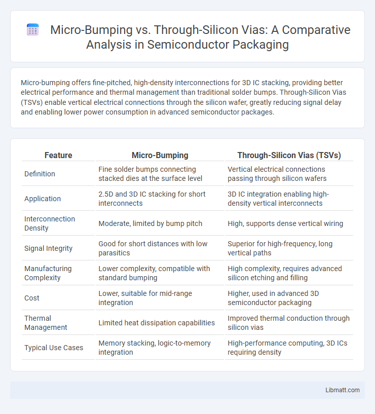
Micro-bumping offers fine-pitched, high-density interconnections for 3D IC stacking, providing better electrical performance and thermal management than traditional solder bumps. Through-Silicon Vias (TSVs) enable vertical electrical connections through the silicon wafer, greatly reducing signal delay and enabling lower power consumption in advanced semiconductor packages.
Table of Comparison
| Feature | Micro-Bumping | Through-Silicon Vias (TSVs) |
|---|---|---|
| Definition | Fine solder bumps connecting stacked dies at the surface level | Vertical electrical connections passing through silicon wafers |
| Application | 2.5D and 3D IC stacking for short interconnects | 3D IC integration enabling high-density vertical interconnects |
| Interconnection Density | Moderate, limited by bump pitch | High, supports dense vertical wiring |
| Signal Integrity | Good for short distances with low parasitics | Superior for high-frequency, long vertical paths |
| Manufacturing Complexity | Lower complexity, compatible with standard bumping | High complexity, requires advanced silicon etching and filling |
| Cost | Lower, suitable for mid-range integration | Higher, used in advanced 3D semiconductor packaging |
| Thermal Management | Limited heat dissipation capabilities | Improved thermal conduction through silicon vias |
| Typical Use Cases | Memory stacking, logic-to-memory integration | High-performance computing, 3D ICs requiring density |
Introduction to Micro-Bumping and Through-Silicon Vias
Micro-bumping enables fine-pitch interconnections by creating small solder bumps, essential for advanced semiconductor packaging and 3D integration. Through-Silicon Vias (TSVs) are vertical electrical connections passing through silicon wafers, facilitating high-density stacking of integrated circuits. Both technologies play critical roles in enhancing performance and reducing form factor in modern electronic devices.
Key Differences Between Micro-Bumping and TSV Technology
Micro-bumping and through-silicon vias (TSVs) are critical interconnect technologies used in advanced semiconductor packaging, differing primarily in their structural scale and application scope. Micro-bumping involves creating tiny solder bumps on chip surfaces for fine-pitch electrical connections in 2.5D and 3D integrated circuits, enabling high-density interposer bonding with reduced parasitic effects. TSV technology, by contrast, fabricates vertical electrical pathways through the silicon wafer, facilitating direct chip stacking for improved signal integrity, thermal performance, and three-dimensional integration in complex systems-on-chip (SoCs).
Structural Design: Micro-Bumping vs. TSV
Micro-bumping features an array of tiny solder bumps on the wafer surface enabling fine-pitch interconnections ideal for high-density packaging, while through-silicon vias (TSVs) are vertical electrical conduits etched through the silicon substrate allowing direct 3D chip stacking with reduced interconnect length. The structural design of micro-bumping involves precise solder ball formation on the die surface facilitating chip-to-chip or chip-to-package connections, whereas TSVs require complex etching, insulation, and filling processes to create vertical channels that improve signal speed and power efficiency. Comparative analysis shows that micro-bumping excels in wafer-level packaging with planar interconnects, whereas TSVs support true 3D integration by enabling vertical stacking and enhanced thermal management.
Performance and Signal Integrity Comparisons
Micro-bumping technology offers superior signal integrity in high-frequency applications due to shorter interconnect paths and reduced parasitic inductance compared to Through-Silicon Vias (TSVs). TSVs excel in vertical integration for 3D ICs, providing higher bandwidth and lower latency by enabling direct, dense inter-layer communication with minimal resistance. Performance trade-offs include micro-bumping's limited vertical scalability versus TSVs' increased complexity and potential signal degradation caused by via-induced capacitance and crosstalk.
Manufacturing Processes of Micro-Bumping and TSV
Micro-bumping manufacturing involves fine pitch solder bump formation directly on chip pads using photolithography and electroplating techniques, enabling high-density interconnects for 3D IC stacking. Through-Silicon Vias (TSVs) require deep silicon etching, dielectric liner deposition, via filling with copper or tungsten, and wafer thinning processes, creating vertical electrical connections through the silicon substrate. Your choice between micro-bumping and TSV depends on device complexity, interconnect density, and thermal management needs in advanced semiconductor packaging.
Cost Implications: Micro-Bumping vs. TSV Integration
Micro-bumping offers a cost-effective solution for high-density interconnects in semiconductor packaging by minimizing material usage and simplifying manufacturing processes. In contrast, Through-Silicon Vias (TSVs) require more complex fabrication steps, including wafer thinning and via etching, significantly increasing production costs. While TSVs provide superior electrical performance and 3D integration, their higher implementation expenses often make micro-bumping the preferred choice for cost-sensitive applications.
Applications and Use Cases in Modern Electronics
Micro-bumping technology is primarily used in high-density interconnects for 3D integrated circuits (ICs) and advanced packaging, enabling fine-pitch connections crucial in mobile devices, high-performance processors, and memory stacks. Through-Silicon Vias (TSVs) facilitate vertical electrical connections through silicon wafers, widely adopted in 3D ICs for heterogeneous integration, such as combining logic and memory chips to enhance speed and power efficiency in data centers and AI accelerators. Both technologies play pivotal roles in modern electronics manufacturing, with micro-bumping favored for ultra-thin form factors, while TSVs excel in high-bandwidth, low-latency applications requiring robust interlayer communication.
Reliability and Thermal Management Considerations
Micro-bumping offers excellent reliability in fine-pitch interconnects but may face challenges with thermal dissipation due to limited contact area. Through-Silicon Vias (TSVs) provide superior thermal management by facilitating efficient heat conduction through the silicon substrate, enhancing overall device performance. Your choice between micro-bumping and TSVs depends on balancing reliability needs against thermal management requirements in advanced packaging designs.
Challenges and Limitations of Both Technologies
Micro-bumping faces challenges such as limited pitch scaling and thermal stress issues, which can affect reliability in high-density interconnects. Through-Silicon Vias (TSVs) encounter limitations including complex fabrication processes, high costs, and potential substrate warping due to deep silicon etching. Your choice between micro-bumping and TSVs should consider these trade-offs in scalability, cost, and mechanical stability for optimal 3D integration performance.
Future Trends in 3D IC Interconnect Technologies
Micro-bumping and Through-Silicon Vias (TSVs) represent key 3D IC interconnect technologies, each advancing towards higher density and improved electrical performance for next-generation devices. Micro-bumping enables fine-pitch connections critical for heterogeneous integration, while TSVs offer vertical interconnects that significantly reduce interconnect length and latency in stacked dies. Your choice between these technologies will depend on application-specific requirements such as signal integrity, thermal management, and scaling potential, driving innovation in future 3D IC architectures.
Micro-Bumping vs Through-Silicon Vias Infographic