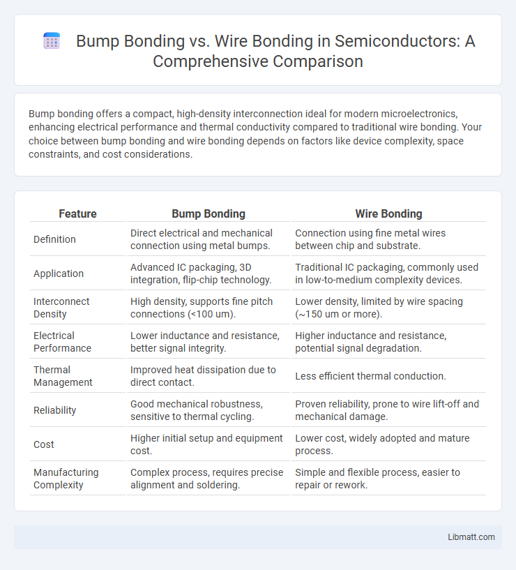
Bump bonding offers a compact, high-density interconnection ideal for modern microelectronics, enhancing electrical performance and thermal conductivity compared to traditional wire bonding. Your choice between bump bonding and wire bonding depends on factors like device complexity, space constraints, and cost considerations.
Table of Comparison
| Feature | Bump Bonding | Wire Bonding |
|---|---|---|
| Definition | Direct electrical and mechanical connection using metal bumps. | Connection using fine metal wires between chip and substrate. |
| Application | Advanced IC packaging, 3D integration, flip-chip technology. | Traditional IC packaging, commonly used in low-to-medium complexity devices. |
| Interconnect Density | High density, supports fine pitch connections (<100 um). | Lower density, limited by wire spacing (~150 um or more). |
| Electrical Performance | Lower inductance and resistance, better signal integrity. | Higher inductance and resistance, potential signal degradation. |
| Thermal Management | Improved heat dissipation due to direct contact. | Less efficient thermal conduction. |
| Reliability | Good mechanical robustness, sensitive to thermal cycling. | Proven reliability, prone to wire lift-off and mechanical damage. |
| Cost | Higher initial setup and equipment cost. | Lower cost, widely adopted and mature process. |
| Manufacturing Complexity | Complex process, requires precise alignment and soldering. | Simple and flexible process, easier to repair or rework. |
Overview of Semiconductor Interconnection Techniques
Bump bonding and wire bonding are critical semiconductor interconnection techniques used to connect integrated circuits (ICs) to substrates or packages, enabling signal transmission and power delivery. Bump bonding involves creating small solder bumps on chip pads for direct vertical connections, offering higher interconnect density, better electrical performance, and reduced parasitic inductance compared to wire bonding. Wire bonding uses fine metal wires to form interconnections between the chip and package leads, providing flexibility and cost-effectiveness, but with limitations in speed and scalability for advanced high-frequency or high-density applications.
What is Bump Bonding?
Bump bonding is an advanced semiconductor packaging technique that creates electrical connections through tiny solder bumps between the chip and the substrate, enabling higher density and better performance than traditional methods. Unlike wire bonding, which relies on thin wires to connect pads, bump bonding provides shorter interconnect paths, reducing signal inductance and improving thermal management. Understanding bump bonding can help you choose the most efficient method for compact and high-speed electronic assemblies.
What is Wire Bonding?
Wire bonding is a widely used method for making electrical connections between a semiconductor device and its packaging using fine metal wires, typically gold, aluminum, or copper. This technique offers reliable performance in microelectronics manufacturing due to its simplicity, cost-effectiveness, and compatibility with various chip designs. Your choice of wire bonding ensures efficient signal transmission and effective thermal management in numerous electronic devices.
Bump Bonding: Key Processes and Materials
Bump bonding involves creating microscopic solder bumps or copper pillars on semiconductor dies using electroplating or printing techniques, enabling direct electrical and mechanical connections to substrates or other dies. Key materials include tin-lead or lead-free solder alloys, copper, and under-bump metallization layers such as nickel and gold that ensure reliable adhesion and conductivity. This process enhances signal integrity and reduces parasitic inductance compared to wire bonding, making it essential for high-performance 3D integrated circuits and advanced packaging solutions.
Wire Bonding: Key Processes and Materials
Wire bonding involves creating electrical interconnections by attaching fine metal wires, typically gold, aluminum, or copper, between semiconductor devices and package leads or substrates. Key processes include thermosonic bonding, thermocompression bonding, and ultrasonic bonding, which rely on heat, pressure, and ultrasonic energy to form reliable mechanical and electrical connections. Materials used in wire bonding must exhibit excellent conductivity, ductility, and bonding strength to ensure optimal device performance and longevity.
Advantages of Bump Bonding
Bump bonding offers superior electrical performance due to its shorter interconnect length, resulting in lower resistance and inductance compared to wire bonding. This method allows for higher input/output (I/O) density and improved thermal management, enhancing the reliability and efficiency of your semiconductor devices. The compact and robust nature of bump bonding is especially advantageous for advanced packaging applications requiring miniaturization and high-speed signal transmission.
Advantages of Wire Bonding
Wire bonding offers several advantages including cost-effectiveness, high reliability, and flexibility in connecting various semiconductor device types. It supports fine pitch connections and allows for easy rework or repair, which enhances manufacturing yields and reduces overall production time. Your choice of wire bonding can lead to improved thermal performance and mechanical stability in electronic packaging.
Limitations and Challenges of Both Methods
Bump bonding faces challenges such as limited scalability for fine-pitch connections and higher sensitivity to thermal stresses, which can cause reliability issues in advanced semiconductor packaging. Wire bonding encounters limitations in speed and signal integrity due to longer interconnect lengths and increased parasitic inductance, making it less suitable for high-frequency applications. Both methods must address cost and complexity trade-offs when integrating with advanced multi-chip modules or 3D IC architectures.
Application Areas: Bump Bonding vs. Wire Bonding
Bump bonding is primarily used in high-density applications such as 3D integrated circuits, advanced packaging, and flip-chip technology, enabling shorter interconnects and improved electrical performance. Wire bonding remains dominant in less dense semiconductor packaging, including microcontrollers, sensors, and power devices, due to its cost-effectiveness and versatility. Your choice between bump bonding and wire bonding depends on the required connection density, electrical performance, and application-specific design constraints.
Future Trends in Microelectronic Bonding Technologies
Future trends in microelectronic bonding technologies emphasize the increasing adoption of bump bonding due to its superior performance in high-density interconnects and enhanced electrical conductivity. Wire bonding remains prevalent for cost-effective and flexible assembly, but innovations in materials and process automation are driving shifts toward finer pitch connections and 3D integration. Your choice between bump bonding and wire bonding will be influenced by evolving demands for miniaturization, reliability, and high-speed data transmission in cutting-edge devices.
Bump Bonding vs Wire Bonding Infographic