SOI CMOS technology offers reduced parasitic capacitance and improved speed compared to bulk CMOS, resulting in lower power consumption and enhanced performance in high-frequency applications. Your choice between SOI and bulk CMOS depends on factors like cost sensitivity, thermal management, and the specific requirements of your electronic design.
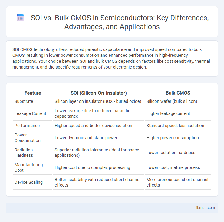
Table of Comparison
| Feature | SOI (Silicon-On-Insulator) | Bulk CMOS |
|---|---|---|
| Substrate | Silicon layer on insulator (BOX - buried oxide) | Silicon wafer (bulk silicon) |
| Leakage Current | Lower leakage due to reduced parasitic capacitance | Higher leakage current |
| Performance | Higher speed and better device isolation | Standard speed, less isolation |
| Power Consumption | Lower dynamic and static power | Higher power consumption |
| Radiation Hardness | Superior radiation tolerance (ideal for space applications) | Lower radiation hardness |
| Manufacturing Cost | Higher cost due to complex processing | Lower cost, mature process |
| Device Scaling | Better scalability with reduced short-channel effects | More pronounced short-channel effects |
Introduction to SOI and Bulk CMOS Technologies
SOI (Silicon-On-Insulator) technology features a layered silicon-insulator-silicon substrate that reduces parasitic capacitance, enhancing device speed and power efficiency compared to Bulk CMOS, which is built directly on a silicon wafer. Bulk CMOS is widely used for its cost-effectiveness and well-established fabrication processes but suffers from higher leakage current and substrate interference. SOI technology offers improved performance for high-speed and low-power applications by minimizing short-channel effects and variability in device characteristics.
Structural Differences between SOI and Bulk CMOS
SOI CMOS features a thin silicon layer separated from the substrate by a buried oxide layer, which reduces parasitic capacitance and improves device isolation. In contrast, Bulk CMOS devices are built directly on the silicon substrate, causing higher junction capacitance and increased leakage currents. The buried oxide in SOI significantly enhances short-channel control and reduces soft errors compared to Bulk CMOS structures.
Device Performance Comparison: SOI vs Bulk CMOS
SOI technology offers superior device performance compared to Bulk CMOS due to reduced parasitic capacitance, which enhances switching speed and lowers power consumption. The high isolation provided by the buried oxide layer in SOI improves short-channel effects and reduces leakage currents, resulting in better overall device reliability. Your designs benefit from SOI's improved thermal characteristics and higher drive currents, making it ideal for high-speed and low-power applications.
Power Consumption: SOI versus Bulk CMOS
SOI (Silicon-On-Insulator) technology significantly reduces power consumption compared to Bulk CMOS by minimizing parasitic capacitance and leakage currents through its insulating layer. This results in lower static power dissipation and improved energy efficiency, especially in low-voltage and high-frequency applications. Bulk CMOS, with its direct substrate connection, typically experiences higher leakage currents, leading to greater power consumption under equivalent operating conditions.
Short-Channel Effects in SOI and Bulk CMOS
Short-channel effects (SCE) manifest differently in SOI versus Bulk CMOS due to their distinct device structures. SOI technology benefits from a buried oxide layer that reduces parasitic capacitance and suppresses drain-induced barrier lowering (DIBL), leading to improved control over short-channel behavior compared to Bulk CMOS. However, floating body effects in SOI can cause variability, whereas Bulk CMOS often experiences increased threshold voltage roll-off and subthreshold leakage as channel lengths scale down.
Fabrication Process Differences
SOI (Silicon-On-Insulator) uses a layered silicon-insulator-silicon substrate that includes a buried oxide layer, reducing parasitic capacitance and improving speed, while bulk CMOS relies on a single silicon wafer with doped regions to form transistors. The SOI fabrication process involves wafer bonding or separation techniques such as SIMOX (Separation by IMplanted OXygen) to create the insulating layer, which adds complexity and cost compared to the more straightforward doping and oxidation steps in bulk CMOS. Your choice of process impacts device performance, power consumption, and manufacturing scalability, with SOI offering advantages in leakage reduction and SOI wafer availability influencing production considerations.
Cost Implications: SOI vs Bulk CMOS
SOI CMOS typically incurs higher manufacturing costs due to the expense of silicon-on-insulator wafers and more complex fabrication processes, impacting overall production budgets. Bulk CMOS benefits from established, cost-efficient fabrication techniques and widely available substrates, making it a more economical choice for high-volume applications. Cost considerations often drive the selection between SOI and Bulk CMOS depending on device performance requirements and market price sensitivity.
Reliability and Longevity
SOI (Silicon-On-Insulator) technology offers enhanced reliability and longevity compared to Bulk CMOS by reducing parasitic capacitance and minimizing dielectric breakdown risks. The buried oxide layer in SOI devices provides better isolation, leading to lower leakage currents and improved tolerance to radiation and temperature variations. Your designs benefit from SOI's superior stability and reduced soft error rates, extending the operational lifespan in demanding applications.
Applications and Use Cases
SOI technology excels in high-performance computing, RF applications, and low-power designs due to its reduced parasitic capacitance and improved speed, making it ideal for mobile devices and aerospace systems. Bulk CMOS remains prevalent in cost-sensitive mass production environments like consumer electronics and automotive applications, where robustness and scalability are crucial. Choosing between SOI and Bulk CMOS aligns with your specific application needs, balancing power efficiency, speed, and manufacturing cost.
Future Trends in SOI and Bulk CMOS Technologies
Future trends in SOI technology emphasize enhanced power efficiency and improved device scaling through advanced ultra-thin body transistors and fully depleted architectures, catering to high-performance computing and low-power applications. Bulk CMOS development is shifting towards innovative doping techniques and strain engineering to sustain Moore's Law, alongside integration with 3D stacking and advanced node manufacturing for cost-effective mass production. Both SOI and Bulk CMOS are converging with emerging materials and heterogeneous integration to enable next-generation semiconductor devices.
SOI vs Bulk CMOS Infographic