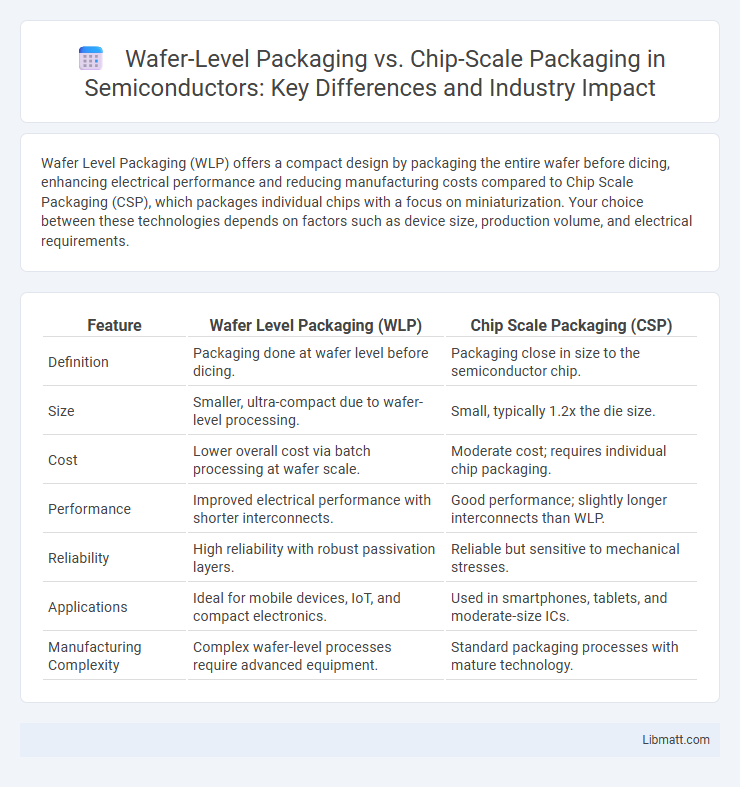
Wafer Level Packaging (WLP) offers a compact design by packaging the entire wafer before dicing, enhancing electrical performance and reducing manufacturing costs compared to Chip Scale Packaging (CSP), which packages individual chips with a focus on miniaturization. Your choice between these technologies depends on factors such as device size, production volume, and electrical requirements.
Table of Comparison
| Feature | Wafer Level Packaging (WLP) | Chip Scale Packaging (CSP) |
|---|---|---|
| Definition | Packaging done at wafer level before dicing. | Packaging close in size to the semiconductor chip. |
| Size | Smaller, ultra-compact due to wafer-level processing. | Small, typically 1.2x the die size. |
| Cost | Lower overall cost via batch processing at wafer scale. | Moderate cost; requires individual chip packaging. |
| Performance | Improved electrical performance with shorter interconnects. | Good performance; slightly longer interconnects than WLP. |
| Reliability | High reliability with robust passivation layers. | Reliable but sensitive to mechanical stresses. |
| Applications | Ideal for mobile devices, IoT, and compact electronics. | Used in smartphones, tablets, and moderate-size ICs. |
| Manufacturing Complexity | Complex wafer-level processes require advanced equipment. | Standard packaging processes with mature technology. |
Introduction to Wafer Level Packaging (WLP) and Chip Scale Packaging (CSP)
Wafer Level Packaging (WLP) involves packaging integrated circuits directly at the wafer level before dicing, enabling reduced package size and improved electrical performance. Chip Scale Packaging (CSP) refers to packaging techniques where the final package size is nearly the same as the semiconductor die, enhancing miniaturization and integration in electronic devices. Both WLP and CSP offer distinct advantages in modern electronics by optimizing space, thermal management, and manufacturing efficiency.
Key Differences Between WLP and CSP
Wafer Level Packaging (WLP) differs from Chip Scale Packaging (CSP) primarily in the stage of application and package size precision; WLP is applied directly to the entire wafer before dicing, enabling smaller, more uniform packages with reduced footprint and enhanced electrical performance. CSP, typically a form of packaging closely matching the chip size, is applied post-dicing and may involve additional substrate layers, resulting in slightly larger dimensions and potentially higher parasitic inductance. The key distinctions include WLP's advantage in miniaturization and high-density integration versus CSP's simplicity and flexibility for less complex assembly processes.
Technological Overview: How WLP Works
Wafer Level Packaging (WLP) involves packaging semiconductor devices directly at the wafer level before dicing, utilizing redistribution layers (RDLs) and solder bumps to create electrical connections. This method enhances miniaturization and improves electrical performance by reducing parasitic inductance and capacitance compared to traditional Chip Scale Packaging (CSP). Your design benefits from WLP's higher precision and thinner profile, making it ideal for compact, high-performance electronics.
Technological Overview: How CSP Works
Chip Scale Packaging (CSP) integrates the die into a package nearly the same size as the chip itself, enhancing electrical performance and enabling higher component density on circuit boards. Wafer Level Packaging (WLP) involves packaging the entire wafer before dicing, applying redistribution layers and solder bumps directly onto the wafer, resulting in reduced package size and improved reliability. Your choice between CSP and WLP affects manufacturing efficiency and device miniaturization, critical for advanced semiconductor applications.
Advantages of Wafer Level Packaging
Wafer Level Packaging (WLP) offers significant advantages such as reduced package size and improved electrical performance by integrating the packaging process directly on the wafer, enhancing signal integrity and reducing parasitic inductance. This method also enables lower manufacturing costs due to batch processing and improved thermal management compared to Chip Scale Packaging (CSP). Your electronic designs benefit from WLP's scalability and reliability in high-density, miniaturized applications where space and performance are critical.
Benefits of Chip Scale Packaging
Chip Scale Packaging (CSP) offers significant advantages including reduced package size closely matching the die dimensions, which enhances electrical performance and thermal management. CSP provides lower inductance and capacitance, resulting in faster signal transmission and improved reliability in high-frequency applications. Its compatibility with automated assembly processes reduces production costs and supports high-volume manufacturing with consistent quality.
Applications and Use Cases of WLP and CSP
Wafer Level Packaging (WLP) is widely used in mobile devices and wearables due to its compact size and excellent electrical performance, making it ideal for high-frequency applications like RF modules and sensors. Chip Scale Packaging (CSP) finds extensive application in consumer electronics and automotive systems where cost-effectiveness and reliable thermal management are crucial, especially in memory devices and microcontrollers. Your choice between WLP and CSP should consider factors like device size, performance requirements, and production volume to optimize application outcomes.
Performance and Reliability Comparison
Wafer Level Packaging (WLP) offers superior electrical performance due to shorter interconnects and reduced parasitic inductance compared to Chip Scale Packaging (CSP), enhancing signal integrity and power efficiency. WLP demonstrates higher reliability in thermal cycling and mechanical stress tests, attributable to its uniform package structure and minimized package size. CSP provides moderate performance benefits but typically shows greater susceptibility to solder joint fatigue and delamination under similar operating conditions.
Cost Analysis: WLP vs. CSP
Wafer Level Packaging (WLP) typically offers lower manufacturing costs due to its streamlined process that integrates packaging at the wafer stage, minimizing material usage and assembly steps. Chip Scale Packaging (CSP), while slightly more expensive, delivers enhanced mechanical stability and easier board-level integration, which can reduce overall system costs but increase upfront expenses. Your choice between WLP and CSP should consider the balance between initial packaging costs and long-term reliability requirements in your specific application.
Future Trends in Advanced Semiconductor Packaging
Future trends in advanced semiconductor packaging emphasize increased integration and miniaturization, with Wafer Level Packaging (WLP) enabling superior electrical performance and cost efficiency by processing at the wafer scale. Chip Scale Packaging (CSP) continues to evolve with enhanced thermal management and higher density interconnections, supporting the demand for compact, high-performance devices. Your choice between WLP and CSP will significantly impact product reliability and scalability in emerging applications like 5G, IoT, and AI-driven systems.
Wafer Level Packaging vs Chip Scale Packaging Infographic