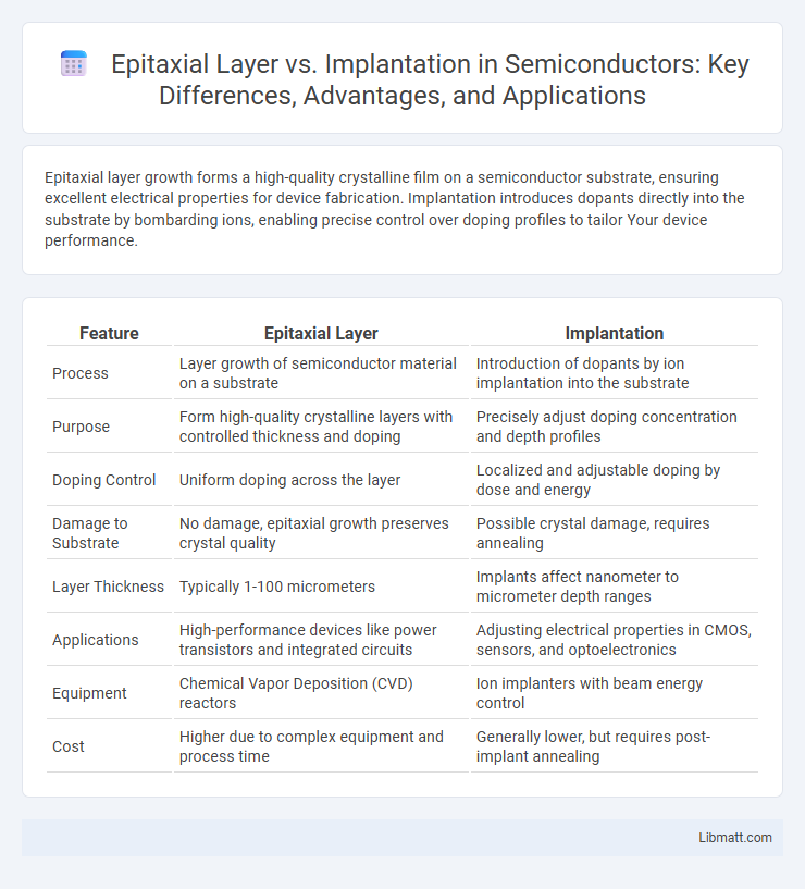
Epitaxial layer growth forms a high-quality crystalline film on a semiconductor substrate, ensuring excellent electrical properties for device fabrication. Implantation introduces dopants directly into the substrate by bombarding ions, enabling precise control over doping profiles to tailor Your device performance.
Table of Comparison
| Feature | Epitaxial Layer | Implantation |
|---|---|---|
| Process | Layer growth of semiconductor material on a substrate | Introduction of dopants by ion implantation into the substrate |
| Purpose | Form high-quality crystalline layers with controlled thickness and doping | Precisely adjust doping concentration and depth profiles |
| Doping Control | Uniform doping across the layer | Localized and adjustable doping by dose and energy |
| Damage to Substrate | No damage, epitaxial growth preserves crystal quality | Possible crystal damage, requires annealing |
| Layer Thickness | Typically 1-100 micrometers | Implants affect nanometer to micrometer depth ranges |
| Applications | High-performance devices like power transistors and integrated circuits | Adjusting electrical properties in CMOS, sensors, and optoelectronics |
| Equipment | Chemical Vapor Deposition (CVD) reactors | Ion implanters with beam energy control |
| Cost | Higher due to complex equipment and process time | Generally lower, but requires post-implant annealing |
Introduction to Epitaxial Layer and Implantation
Epitaxial layer refers to a thin, single-crystal semiconductor film grown on a substrate wafer, essential for enhancing device performance in semiconductor manufacturing. Implantation involves bombarding a semiconductor wafer with high-energy ions to modify electrical properties through precise dopant distribution. Both techniques are fundamental in fabricating integrated circuits, with epitaxial layers providing high-quality crystalline surfaces and implantation enabling controlled doping profiles.
Fundamental Differences Between Epitaxy and Implantation
Epitaxial layer growth involves depositing a single-crystal semiconductor layer on a substrate to create a high-quality, defect-free crystalline structure essential for device performance. Implantation, by contrast, entails bombarding the substrate with high-energy ions to introduce dopants or modify material properties without altering the crystal lattice's continuity. The fundamental difference lies in epitaxy building new crystalline layers epitaxially matched to the substrate, whereas implantation alters the substrate's chemical composition through ion penetration and lattice damage.
Epitaxial Layer Formation: Process and Materials
Epitaxial layer formation involves depositing a single-crystal semiconductor layer on a substrate, typically silicon, using chemical vapor deposition (CVD) processes to ensure lattice alignment and high-quality crystal growth. This method uses precursor gases like silane or dichlorosilane in a controlled temperature environment to form uniform, defect-free epitaxial layers essential for advanced semiconductor devices. Your choice of epitaxial layer materials and precise process parameters directly impacts device performance by enhancing carrier mobility and reducing defects compared to ion implantation techniques.
Ion Implantation Technique: Process Overview
Ion implantation is a precise semiconductor doping technique where ions are accelerated and embedded into the substrate to modify electrical properties, offering controlled depth and concentration profiles. Unlike epitaxial layer growth, which deposits a crystalline layer on the substrate, ion implantation allows for targeted doping without altering the surface morphology. This process is critical in fabricating integrated circuits, enabling precise formation of p-n junctions and device structures.
Structural Properties: Epitaxial Layers vs Implanted Layers
Epitaxial layers exhibit highly ordered crystal structures with minimal defects, as they grow atom-by-atom aligned to the substrate lattice, ensuring superior structural integrity. Implanted layers, however, introduce significant lattice damage and disorder due to ion bombardment, often requiring subsequent annealing to partially restore crystallinity. Your choice between epitaxial growth and ion implantation impacts device performance by balancing pristine crystal quality against doping precision and depth control.
Electrical Characteristics Comparison
Epitaxial layers provide superior electrical characteristics such as higher carrier mobility and lower defect density, resulting in improved current flow and device reliability compared to implantation. Ion implantation introduces dopants directly but can cause crystal damage and increased leakage current, affecting device performance. Your choice between epitaxial layer growth and implantation depends on the required electrical properties and precision in semiconductor device fabrication.
Applications in Semiconductor Devices
Epitaxial layer growth enables the formation of high-purity, defect-free semiconductor substrates essential for high-performance devices like power transistors and integrated circuits. Ion implantation precisely dopes semiconductor regions to create p-n junctions with controlled electrical properties in devices such as CMOS transistors and diodes. Both techniques are critical in tailoring the electrical characteristics and enhancing the functionality of modern semiconductor components.
Advantages and Limitations of Epitaxial Layers
Epitaxial layers provide superior crystal quality and uniformity, enabling enhanced electrical performance and precise control of thickness essential for advanced semiconductor devices. These layers exhibit excellent interface properties and reduced defects compared to implantation, making them ideal for high-frequency and power applications. You should consider limitations such as higher production costs and complexity, as well as challenges in doping control compared to ion implantation techniques.
Advantages and Drawbacks of Ion Implantation
Ion implantation offers precise control over dopant concentration and depth profiles, enabling uniform and reproducible semiconductor device fabrication. The technique minimizes thermal budget since it operates at relatively low temperatures compared to epitaxial growth, reducing unwanted diffusion and defects. However, ion implantation can introduce crystal damage and require annealing steps to restore semiconductor lattice quality, potentially complicating process integration.
Future Trends in Doping Techniques
Advanced doping techniques like epitaxial layer growth and ion implantation are evolving to meet the demand for smaller, more efficient semiconductor devices. Future trends indicate a shift towards atomic-level precision doping through methods such as plasma-enhanced epitaxy and ultra-low energy implantation, enabling better control of dopant distribution and reduced defects. Your ability to harness these cutting-edge techniques will be crucial for developing next-generation integrated circuits with enhanced performance and reliability.
Epitaxial Layer vs Implantation Infographic