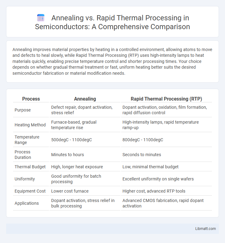
Annealing improves material properties by heating in a controlled environment, allowing atoms to move and defects to heal slowly, while Rapid Thermal Processing (RTP) uses high-intensity lamps to heat materials quickly, enabling precise temperature control and shorter processing times. Your choice depends on whether gradual thermal treatment or fast, uniform heating better suits the desired semiconductor fabrication or material modification needs.
Table of Comparison
| Process | Annealing | Rapid Thermal Processing (RTP) |
|---|---|---|
| Purpose | Defect repair, dopant activation, stress relief | Dopant activation, oxidation, film formation, rapid diffusion control |
| Heating Method | Furnace-based, gradual temperature rise | High-intensity lamps, rapid temperature ramp-up |
| Temperature Range | 500degC - 1100degC | 800degC - 1100degC |
| Process Duration | Minutes to hours | Seconds to minutes |
| Thermal Budget | High, longer heat exposure | Low, minimal thermal budget |
| Uniformity | Good uniformity for batch processing | Excellent uniformity on single wafers |
| Equipment Cost | Lower cost furnace | Higher cost, advanced RTP tools |
| Applications | Dopant activation, stress relief in bulk processing | Advanced CMOS fabrication, rapid dopant activation |
Introduction to Annealing and Rapid Thermal Processing
Annealing is a thermal treatment process that involves heating a material to a specific temperature to alter its physical and chemical properties, such as reducing hardness and increasing ductility. Rapid Thermal Processing (RTP) rapidly heats the wafer to high temperatures for short durations, enabling precise control over diffusion processes and minimizing thermal budget. Both techniques are essential in semiconductor manufacturing, with annealing commonly used for stress relief and defect reduction, while RTP is favored for ultrafast thermal cycles in advanced device fabrication.
Fundamental Principles of Annealing
Annealing involves heating a material to a specific temperature to alter its microstructure, reduce defects, and improve mechanical properties such as ductility and hardness. This process relies on diffusion mechanisms that allow atoms to move and reconfigure, relieving internal stresses and facilitating grain growth. Unlike Rapid Thermal Processing (RTP), which uses short, high-temperature pulses for wafer treatment, traditional annealing provides slower thermal exposure, enabling controlled phase transformations and structural stabilization.
Key Concepts Behind Rapid Thermal Processing
Rapid Thermal Processing (RTP) uses intense, short bursts of infrared light to heat semiconductor wafers quickly, enabling precise control over thermal cycles critical for processes like dopant activation and oxide growth. Unlike traditional annealing, which heats wafers for extended periods, RTP minimizes thermal budget and diffusion effects, preserving device integrity and improving performance. Your semiconductor manufacturing benefits from RTP by achieving rapid temperature ramp-up and cool-down rates, enhancing throughput and ensuring uniform thermal treatment.
Temperature Profiles: Annealing vs RTP
Annealing involves a sustained temperature profile typically ranging from 600degC to 1100degC held for several minutes to hours, allowing gradual diffusion and defect repair in semiconductor materials. Rapid Thermal Processing (RTP) uses a quick temperature ramp-up to peak temperatures as high as 1150degC within seconds, followed by rapid cooling, minimizing diffusion and enabling precise dopant activation. The controlled, extended heating in annealing contrasts sharply with the short, intense thermal spikes of RTP, impacting material properties and device performance differently.
Process Duration and Efficiency Comparison
Annealing typically involves longer process durations ranging from several minutes to hours, enabling thorough thermal diffusion and defect reduction in semiconductor materials. Rapid Thermal Processing (RTP) significantly shortens process times to mere seconds or minutes by using high-intensity lamps for fast temperature ramp-up and cooldown, enhancing throughput and reducing thermal budget. The efficiency of RTP lies in minimizing thermal exposure, which decreases undesired diffusion while maintaining effective activation of dopants, whereas annealing prioritizes uniformity but at the cost of longer cycle times.
Material Applications and Suitability
Annealing is widely used for improving the crystallinity and reducing defects in semiconductor materials like silicon and germanium, making it suitable for applications requiring uniform thermal treatment and deeper diffusion profiles. Rapid Thermal Processing (RTP) is preferred for precise, short-duration heat treatments in advanced devices such as CMOS transistors and high-k dielectrics, where minimal thermal budget and sharp temperature control are critical. Your choice between annealing and RTP depends on the material compatibility and the thermal requirements of the fabrication process, balancing throughput and device performance.
Effects on Microstructure and Material Properties
Annealing promotes grain growth and reduces dislocations, enhancing ductility and reducing internal stresses in materials, while Rapid Thermal Processing (RTP) controls grain size more precisely by limiting diffusion due to its short, high-temperature cycles. The microstructure resulting from annealing typically exhibits larger grains and improved electrical properties, whereas RTP preserves fine microstructures, leading to superior hardness and wear resistance. Your choice between these methods impacts mechanical strength, electrical conductivity, and overall material performance based on target application requirements.
Advantages and Limitations of Annealing
Annealing offers advantages such as improved crystal quality, reduced defects, and enhanced electrical properties due to its controlled, uniform heating typically conducted over longer durations. Limitations of annealing include longer processing times, potential diffusion of dopants leading to less precise control, and higher thermal budgets compared to rapid thermal processing. Your choice of annealing depends on the need for uniformity and crystal repair versus speed and dopant profile control.
Benefits and Drawbacks of Rapid Thermal Processing
Rapid Thermal Processing (RTP) enables precise control of temperature ramp rates and short annealing times, minimizing diffusion and enhancing dopant activation in semiconductor manufacturing. RTP offers benefits such as reduced thermal budget, improved junction abruptness, and compatibility with advanced device architectures, but drawbacks include higher equipment costs, process complexity, and potential wafer stress from rapid heating and cooling cycles. Compared to conventional annealing, RTP's rapid cycles improve throughput and reduce contamination risks, yet require careful thermal management to avoid non-uniformities and defect generation.
Selecting the Right Process: Factors to Consider
Selecting the right process between Annealing and Rapid Thermal Processing depends on factors such as thermal budget, wafer throughput, and specific material requirements. Annealing is ideal for applications needing slower, uniform heating to repair crystal defects, while Rapid Thermal Processing offers quicker temperature ramp-up and precise thermal cycles for dopant activation and oxide growth. Key considerations include process speed, temperature uniformity, equipment cost, and desired impact on semiconductor device performance.
Annealing vs Rapid Thermal Processing Infographic