Edge bead removal ensures the uniform application of photoresist by eliminating excess material along the wafer edges, preventing defects during semiconductor fabrication. Your process benefits from spin rinse dry by effectively cleaning and drying wafers, maintaining surface integrity without introducing contaminants or damage.
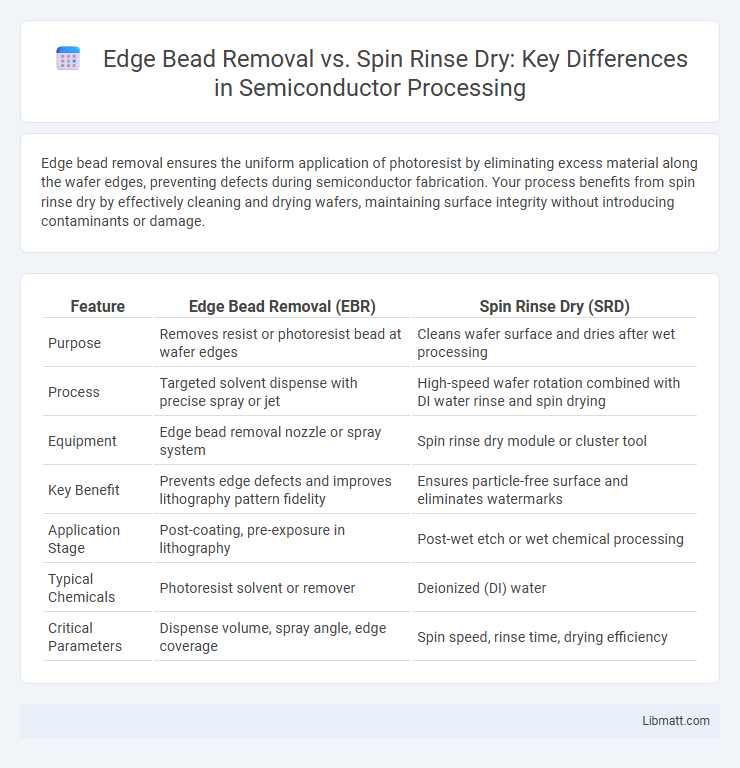
Table of Comparison
| Feature | Edge Bead Removal (EBR) | Spin Rinse Dry (SRD) |
|---|---|---|
| Purpose | Removes resist or photoresist bead at wafer edges | Cleans wafer surface and dries after wet processing |
| Process | Targeted solvent dispense with precise spray or jet | High-speed wafer rotation combined with DI water rinse and spin drying |
| Equipment | Edge bead removal nozzle or spray system | Spin rinse dry module or cluster tool |
| Key Benefit | Prevents edge defects and improves lithography pattern fidelity | Ensures particle-free surface and eliminates watermarks |
| Application Stage | Post-coating, pre-exposure in lithography | Post-wet etch or wet chemical processing |
| Typical Chemicals | Photoresist solvent or remover | Deionized (DI) water |
| Critical Parameters | Dispense volume, spray angle, edge coverage | Spin speed, rinse time, drying efficiency |
Introduction to Edge Bead Removal and Spin Rinse Dry
Edge Bead Removal (EBR) is a critical process in semiconductor manufacturing that eliminates excess photoresist from wafer edges to ensure uniform coating and prevent defects during subsequent lithography steps. Spin Rinse Dry (SRD) combines spin drying with rinsing to efficiently remove contaminants and photoresist residues from wafer surfaces while ensuring rapid drying to avoid watermarks. Understanding the differences between EBR and SRD helps optimize wafer surface preparation, improving yield and device performance in your fabrication process.
Understanding Edge Bead Formation in Semiconductor Processing
Edge bead formation occurs during semiconductor wafer coating when excess photoresist accumulates at the wafer's edge, leading to thickness nonuniformities that can compromise lithography accuracy. Edge Bead Removal (EBR) techniques effectively eliminate this excess material, ensuring uniform layer thickness crucial for precise patterning. Spin Rinse Dry (SRD) processes complement EBR by cleaning and drying the wafer surface, but only EBR directly addresses edge bead, which is essential for your semiconductor device's yield and performance.
Principles of Edge Bead Removal (EBR) Techniques
Edge Bead Removal (EBR) techniques operate by selectively eliminating excess photoresist buildup at the wafer's edges to prevent defects during lithographic processing. Common methods include plasma etching, solvent-based removal, and mechanical edge scrubbing, each optimizing the wafer surface for uniform coating and accurate patterning. Precise control of process parameters such as gas flow, exposure time, and chemical concentration ensures effective edge bead removal while minimizing substrate damage.
Overview of Spin Rinse Dry (SRD) Processes
Spin Rinse Dry (SRD) processes utilize centrifugal force to remove excess liquids and contaminants from semiconductor wafers, enabling thorough cleaning without mechanical contact. SRD systems rotate wafers at high speeds while simultaneously spraying ultra-pure water, ensuring uniform rinsing and drying that prevents recontamination. Edge Bead Removal (EBR) focuses on eliminating resist buildup on wafer edges, but SRD offers a comprehensive final cleanse essential for defect minimization in photolithography.
Key Differences Between EBR and SRD Methods
Edge Bead Removal (EBR) targets the removal of excess photoresist from the wafer edges using precise solvent application, ensuring uniform coating in semiconductor manufacturing. Spin Rinse Dry (SRD) involves spinning wafers at high speeds while spraying deionized water and drying with nitrogen, effectively cleaning and drying the wafer surface. Unlike EBR, which focuses on defect prevention at wafer edges, SRD emphasizes contaminant removal and drying of the entire wafer surface.
Advantages and Limitations of Edge Bead Removal
Edge Bead Removal (EBR) offers precise elimination of excess photoresist at the wafer edge, improving coating uniformity and preventing defects during photolithography. This process enhances yield by reducing particle contamination and enabling better subsequent processing, but it may introduce complexity and increase cycle time compared to Spin Rinse Dry (SRD) methods. Your choice between EBR and SRD should consider factors like wafer size, photoresist type, and production throughput requirements.
Benefits and Drawbacks of Spin Rinse Dry
Spin rinse dry offers efficient wafer cleaning and drying in a single automated process, reducing manual handling and contamination risk. The technique ensures uniform drying, minimizing watermarks and residues that may impact subsequent photolithography steps. However, its effectiveness may be limited by wafer size and geometry, and improper settings can cause particle redeposition or mechanical stress on delicate wafers.
Applications and Use Cases in Semiconductor Manufacturing
Edge Bead Removal (EBR) is crucial in semiconductor manufacturing for preventing defects during photolithography by eliminating excess photoresist at wafer edges, ensuring uniform coating and improving yield in advanced node device fabrication. Spin Rinse Dry (SRD) is applied post-etching or deposition processes to thoroughly clean wafers, removing particles and chemical residues while drying the surface without watermarks, critical for maintaining surface integrity in IC production. EBR is primarily used during resist coating to enhance pattern fidelity, whereas SRD supports various stages including cleaning and post-process treatment, both integral to achieving high-quality semiconductor device fabrication.
Process Integration: Choosing Between EBR and SRD
Edge Bead Removal (EBR) and Spin Rinse Dry (SRD) integrate differently into semiconductor fabrication lines, with EBR specifically targeting the removal of resist beads to prevent defects during photolithography. SRD combines rinsing and drying in a single step, optimizing wafer throughput and reducing contamination risk in post-etch cleaning. Selection depends on process requirements: EBR suits precise resist patterning control, while SRD enhances overall cycle efficiency and cleanliness.
Future Trends in Wafer Cleaning and Edge Processing Technologies
Future trends in wafer cleaning emphasize advanced Edge Bead Removal (EBR) techniques that enhance uniformity and reduce defects at the wafer periphery. Spin Rinse Dry (SRD) systems are evolving with improved fluid dynamics and drying mechanisms to increase throughput and minimize particle contamination. Your semiconductor manufacturing process will benefit from integrating these cutting-edge technologies to boost yield and ensure cleaner wafer surfaces.
Edge Bead Removal vs Spin Rinse Dry Infographic