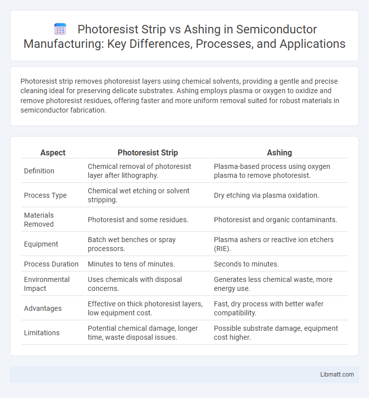
Photoresist strip removes photoresist layers using chemical solvents, providing a gentle and precise cleaning ideal for preserving delicate substrates. Ashing employs plasma or oxygen to oxidize and remove photoresist residues, offering faster and more uniform removal suited for robust materials in semiconductor fabrication.
Table of Comparison
| Aspect | Photoresist Strip | Ashing |
|---|---|---|
| Definition | Chemical removal of photoresist layer after lithography. | Plasma-based process using oxygen plasma to remove photoresist. |
| Process Type | Chemical wet etching or solvent stripping. | Dry etching via plasma oxidation. |
| Materials Removed | Photoresist and some residues. | Photoresist and organic contaminants. |
| Equipment | Batch wet benches or spray processors. | Plasma ashers or reactive ion etchers (RIE). |
| Process Duration | Minutes to tens of minutes. | Seconds to minutes. |
| Environmental Impact | Uses chemicals with disposal concerns. | Generates less chemical waste, more energy use. |
| Advantages | Effective on thick photoresist layers, low equipment cost. | Fast, dry process with better wafer compatibility. |
| Limitations | Potential chemical damage, longer time, waste disposal issues. | Possible substrate damage, equipment cost higher. |
Introduction to Photoresist Removal
Photoresist removal is a crucial step in semiconductor fabrication that ensures clean and defect-free surfaces for subsequent processing. Photoresist strip involves the use of chemical solvents to dissolve and remove the photoresist layer, while ashing employs plasma etching to oxidize and vaporize the photoresist material. Understanding the differences between these methods helps optimize your semiconductor manufacturing yield and enhances device performance.
What Is Photoresist Strip?
Photoresist strip is a chemical process used to remove photoresist material from semiconductor wafers after lithography steps, ensuring a clean surface for subsequent fabrication stages. Unlike ashing, which relies on plasma to oxidize and strip photoresist, the photoresist strip uses solvent-based or aqueous chemicals tailored to dissolve the resist without damaging the underlying layers. Your semiconductor manufacturing quality and efficiency depend on selecting the appropriate stripping method to prevent contamination and maintain device integrity.
Understanding Ashing in Semiconductor Processing
Ashing in semiconductor processing refers to the plasma-based removal of photoresist materials by converting them into gaseous byproducts using reactive oxygen species. This method offers precise control over the stripping process, minimizing damage to underlying substrates compared to wet chemical photoresist strip techniques. You can achieve higher purity and cleaner surfaces with ashing, which is critical for advanced semiconductor device fabrication.
Chemical vs Plasma-Based Removal Methods
Photoresist strip utilizes chemical solvents or alkaline solutions to dissolve and remove the photoresist layer, offering precise control over chemical interactions but often requiring longer processing times and careful waste management. Ashing, a plasma-based removal method, employs oxygen or fluorine-containing plasma to oxidize and volatilize organic photoresist materials rapidly, enabling high-throughput processing and compatibility with complex topographies. The choice between chemical strip and plasma ashing depends on factors such as substrate sensitivity, throughput demands, and environmental considerations in semiconductor fabrication.
Key Equipment Used in Strip and Ashing
Photoresist strip processes primarily utilize wet chemical scrubbers and solvent-based spin coaters designed to gently dissolve and remove photoresist layers without damaging the substrate. Ashing equipment, on the other hand, relies on plasma etchers that generate oxygen or fluorine-based plasmas to oxidize and etch away the photoresist, offering precise and residue-free removal. Selecting the right equipment for your photoresist removal depends on the specific requirements of your semiconductor fabrication or PCB manufacturing process.
Process Efficiency: Strip vs Ashing
Photoresist strip offers higher process efficiency by quickly removing thick photoresist layers with minimal substrate damage using chemical solvents. Ashing, typically a plasma-based process, provides more precise removal of residual photoresist, especially in hard-to-reach areas, but generally requires longer processing times. Optimizing the choice between strip and ashing depends on balancing throughput needs with sensitivity to substrate materials in semiconductor fabrication.
Impact on Substrate Integrity
Photoresist strip processes use chemical solvents that can gently remove photoresist while preserving substrate integrity, minimizing mechanical or thermal stress. Ashing employs plasma to oxidize and vaporize photoresist, which may introduce substrate roughness or damage due to ion bombardment and heat. Choosing the right method depends on your substrate's sensitivity and the desired balance between efficiency and surface preservation.
Environmental and Safety Considerations
Photoresist strip typically involves the use of chemical solvents which can pose hazards related to toxicity, flammability, and disposal, requiring proper ventilation and waste management to minimize environmental impact. Ashing uses oxygen plasma to remove photoresist, producing fewer hazardous chemical wastes but necessitating strict controls to prevent exposure to ozone and other reactive gases. Your choice between the two should consider facility capabilities for handling chemical safety protocols or plasma exhaust systems to ensure environmental compliance and worker protection.
Cost Comparison of Strip and Ashing Methods
Photoresist strip methods typically incur higher chemical costs due to the use of specialized solvents, while ashing processes often require significant energy consumption and maintenance for plasma generation equipment. Strip techniques usually involve longer processing times, increasing operational expenses, whereas ashing offers faster throughput but may demand costly system infrastructure. Evaluating total cost requires balancing chemical and utility expenses in strip methods against capital investment and upkeep in ashing technology.
Choosing the Right Method for Your Application
Choosing the right method for photoresist removal depends on your specific application requirements, including substrate sensitivity and process precision. Photoresist strip uses chemical solvents to dissolve the resist, offering compatibility with delicate materials but requiring careful handling of chemicals. Ashing employs plasma to etch away the resist, providing a dry, residue-free finish suitable for high-throughput semiconductor fabrication, making it essential to evaluate material compatibility and process integration for optimal results.
Photoresist Strip vs Ashing Infographic

 libmatt.com