Gate Last technology places the gate electrode after source/drain formation, allowing for better strain engineering and improved transistor performance, while Gate First involves creating the gate before source/drain implantation, offering simpler processing and reduced gate damage. Your choice between Gate Last and Gate First impacts device scalability, electrical characteristics, and manufacturing complexity in semiconductor fabrication.
Table of Comparison
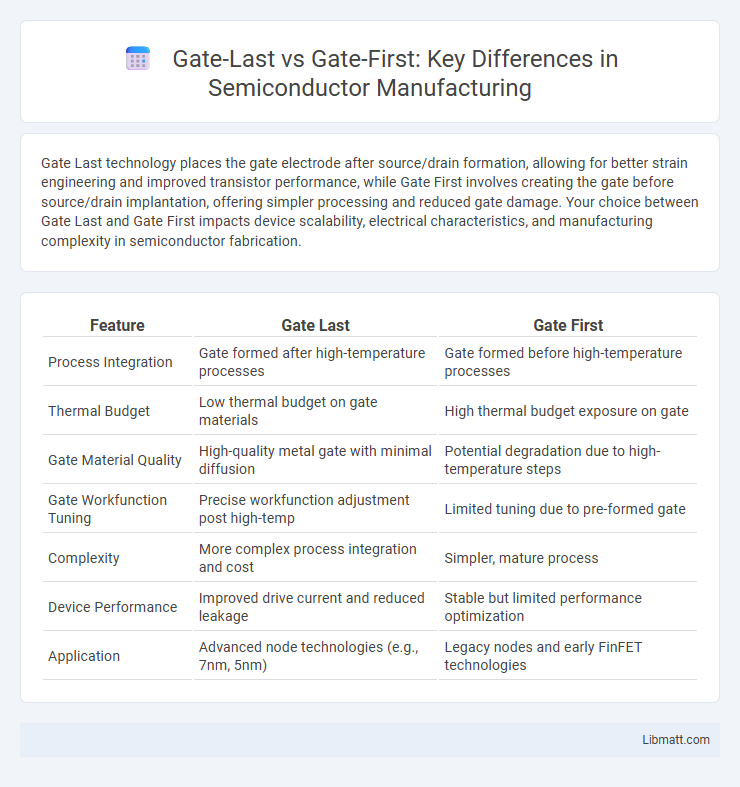
| Feature | Gate Last | Gate First |
|---|---|---|
| Process Integration | Gate formed after high-temperature processes | Gate formed before high-temperature processes |
| Thermal Budget | Low thermal budget on gate materials | High thermal budget exposure on gate |
| Gate Material Quality | High-quality metal gate with minimal diffusion | Potential degradation due to high-temperature steps |
| Gate Workfunction Tuning | Precise workfunction adjustment post high-temp | Limited tuning due to pre-formed gate |
| Complexity | More complex process integration and cost | Simpler, mature process |
| Device Performance | Improved drive current and reduced leakage | Stable but limited performance optimization |
| Application | Advanced node technologies (e.g., 7nm, 5nm) | Legacy nodes and early FinFET technologies |
Introduction to Gate Last and Gate First Technologies
Gate Last and Gate First technologies represent two distinct approaches in semiconductor manufacturing. Gate First integrates the gate electrode before high-temperature processing, offering better control of gate dimensions but facing challenges with gate oxide integrity. Gate Last, also known as Replacement Metal Gate (RMG), forms the gate after high-temperature steps, allowing for improved material properties and performance, which can enhance Your chip's overall efficiency and scalability.
Understanding the Gate Stack Process
Gate Last and Gate First represent two distinct approaches in semiconductor manufacturing related to the formation of the gate stack in transistors. Gate First integrates the high-k/metal gate materials early in the process before source/drain engineering, enabling better thermal stability but facing challenges with dopant diffusion. Gate Last, also known as replacement metal gate (RMG), involves forming a dummy gate initially and replacing it with the final gate stack after high-temperature steps, improving gate material quality and performance for advanced technology nodes like FinFETs.
Key Differences Between Gate Last and Gate First
Gate Last technology integrates the high-k metal gate process after forming the transistor gate dielectric, enabling improved channel mobility and scalable threshold voltage tuning. Gate First process forms the metal gate before high-temperature annealing, leading to challenges in metal gate composition stability but simplified manufacturing steps. The key differences revolve around process timing for gate formation, impact on device performance, and thermal budget flexibility.
Advantages of the Gate Last Approach
The Gate Last approach offers significant advantages in semiconductor manufacturing by enabling greater flexibility in process integration and reducing thermal budget constraints, which preserves the integrity of the high-k metal gate materials. This method allows you to optimize the gate stack independently of the high-temperature front-end processes, leading to improved device performance and scalability in advanced CMOS technologies. Enhanced control over gate dimensions and improved threshold voltage tuning are critical benefits that make Gate Last preferable for cutting-edge transistor designs.
Benefits of the Gate First Method
The Gate First method involves patterning the gate electrode before the source and drain, offering precise control over channel length and improved device scaling. This approach enhances gate oxide integrity and reduces parasitic capacitance, leading to better electrical performance and lower power consumption. You benefit from increased manufacturing yield and reliability due to minimized process variability and improved interface quality.
Process Challenges and Solutions
Gate Last and Gate First approaches present distinct process challenges in semiconductor manufacturing, with Gate Last often encountering stress and integration complexities during high-temperature steps, while Gate First struggles with gate dielectric stability and patterning precision. Solutions for Gate Last involve advanced stress engineering and low thermal budget processes to maintain device performance, whereas Gate First benefits from refined lithography and etch techniques to enhance gate integrity. Your fabrication strategy must weigh these factors to optimize yield and device reliability effectively.
Impact on Device Performance and Scaling
Gate Last technology offers better control over short channel effects and boosts device performance by enabling high-k/metal gate integration after high-temperature processing, while Gate First may suffer from mobility degradation due to high-temperature steps after gate formation. Gate Last facilitates improved scaling by allowing optimized materials and processes for the gate stack, contributing to enhanced electrostatics and reduced leakage currents. Your choice between Gate Last and Gate First impacts the balance between process complexity, device reliability, and scaling potential in advanced semiconductor manufacturing.
Cost Implications in Manufacturing
Gate Last packaging typically incurs higher manufacturing costs due to additional process steps and equipment needed to create dual-layer structures, increasing material and labor expenses. Gate First methods streamline production by integrating the gate during initial molding, reducing cycle times and lowering overall cost per unit. Your choice between Gate Last and Gate First directly impacts budget allocation for tooling, materials, and assembly efficiency.
Industry Trends and Adoption Rates
Gate Last technology, favored for its cost efficiency and yield improvement, is rapidly gaining traction in advanced semiconductor manufacturing, particularly within logic chip production and memory devices. Market analysis indicates a steady increase in adoption rates among leading foundries such as TSMC and Samsung, driven by its compatibility with advanced node scaling and reduced process complexity. Conversely, Gate First remains prevalent in mature technology nodes and niche applications due to its established process stability and integration with high-k metal gate materials.
Future Outlook for Gate Stack Technologies
Gate Last technology offers superior flexibility for integrating high-k/metal gate stacks with advanced node transistors, enabling better control over channel performance and reduced gate leakage for future devices. Gate First processes provide cost efficiency and mature manufacturing steps but may face limitations scaling with emerging 3D transistor architectures and aggressive gate dielectric scaling. Your choice between Gate Last and Gate First impacts long-term scalability, as Gate Last is increasingly favored for next-generation logic and memory devices requiring robust gate stack engineering and enhanced electrostatic integrity.
Gate Last vs Gate First Infographic