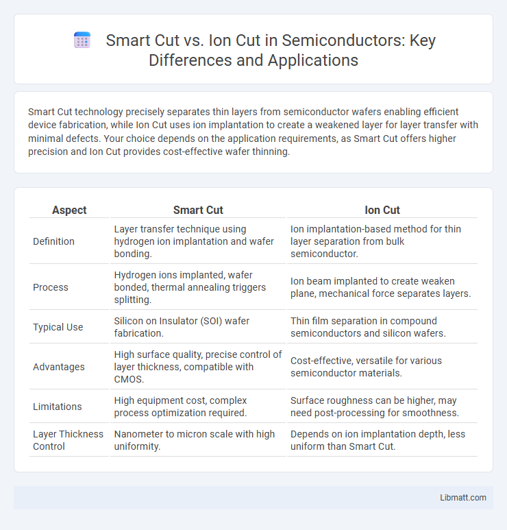
Smart Cut technology precisely separates thin layers from semiconductor wafers enabling efficient device fabrication, while Ion Cut uses ion implantation to create a weakened layer for layer transfer with minimal defects. Your choice depends on the application requirements, as Smart Cut offers higher precision and Ion Cut provides cost-effective wafer thinning.
Table of Comparison
| Aspect | Smart Cut | Ion Cut |
|---|---|---|
| Definition | Layer transfer technique using hydrogen ion implantation and wafer bonding. | Ion implantation-based method for thin layer separation from bulk semiconductor. |
| Process | Hydrogen ions implanted, wafer bonded, thermal annealing triggers splitting. | Ion beam implanted to create weaken plane, mechanical force separates layers. |
| Typical Use | Silicon on Insulator (SOI) wafer fabrication. | Thin film separation in compound semiconductors and silicon wafers. |
| Advantages | High surface quality, precise control of layer thickness, compatible with CMOS. | Cost-effective, versatile for various semiconductor materials. |
| Limitations | High equipment cost, complex process optimization required. | Surface roughness can be higher, may need post-processing for smoothness. |
| Layer Thickness Control | Nanometer to micron scale with high uniformity. | Depends on ion implantation depth, less uniform than Smart Cut. |
Introduction to Smart Cut and Ion Cut Technologies
Smart Cut technology involves a precise layer transfer process using hydrogen implantation and wafer bonding to create ultra-thin semiconductor layers, enhancing device performance and manufacturing yield. Ion Cut refers specifically to the ion implantation step in Smart Cut, where ions are embedded at a controlled depth to facilitate wafer splitting. Your choice between these methods depends on the specific semiconductor application and the desired thin-layer quality.
Principles Behind Smart Cut and Ion Cut Methods
Smart Cut technology involves implanting hydrogen ions into a silicon wafer to create a weakened plane, enabling precise wafer splitting and thin layer transfer for semiconductor fabrication. Ion Cut relies on ion implantation to induce a cleavage plane within the substrate, facilitating layer transfer through controlled exfoliation. Both methods optimize material utilization and surface quality, enhancing device performance and manufacturing efficiency in microelectronics.
Material Applications: Where Each Method Excels
Smart Cut technology excels in producing high-quality silicon-on-insulator (SOI) wafers, ideal for advanced semiconductor devices and microelectromechanical systems (MEMS). Ion Cut is preferred for precise layer transfer in materials like silicon carbide and gallium nitride, essential for power electronics and radio frequency applications. Your choice depends on the specific substrate and device requirements, with Smart Cut offering superior uniformity for silicon-based materials and Ion Cut providing flexibility for diverse compound semiconductors.
Process Workflow: Step-by-Step Comparison
Smart Cut involves hydrogen ion implantation to create a weakened layer within a silicon wafer, followed by wafer bonding and thermal splitting to transfer a thin silicon layer onto a substrate. Ion Cut, similarly, uses ion implantation--but varies in ion species and energy parameters--to induce controlled wafer cleavage, enabling precise layer transfer with minimal surface damage. Your choice between these methods depends on desired layer thickness, surface quality, and application-specific requirements in semiconductor fabrication.
Precision and Surface Quality Differences
Smart Cut technology employs hydrogen ion implantation to enable wafer splitting with exceptional precision, minimizing surface roughness and reducing the need for extensive polishing. Ion Cut, while also using ion implantation, typically results in a slightly rougher cleaved surface, demanding additional surface treatment to achieve comparable smoothness. The enhanced control in Smart Cut yields superior surface quality, making it ideal for advanced semiconductor layer transfer applications.
Scalability and Manufacturing Efficiency
Smart Cut technology offers superior scalability by enabling precise layer transfer with minimal material waste, facilitating large-scale production of thin semiconductor wafers. Ion Cut provides manufacturing efficiency through a well-established process that allows high throughput and reliable wafer splitting but can face limitations in scaling up for ultra-thin substrates. Choosing between these methods depends on your production volume needs and the desired balance between cost-efficiency and wafer quality.
Cost Implications of Smart Cut vs Ion Cut
Smart Cut technology typically incurs higher initial costs due to complex wafer bonding and splitting processes, but offers superior precision and reduced material waste, leading to long-term cost savings in semiconductor manufacturing. Ion Cut, while generally cheaper upfront with simpler implantation and exfoliation steps, may result in higher defect rates and additional processing for surface planarization, increasing overall expenses. Evaluating these cost implications requires balancing immediate capital investment against yield efficiency and product quality in semiconductor fabrication.
Environmental and Safety Considerations
Smart Cut technology minimizes material waste and reduces the use of hazardous chemicals compared to Ion Cut, making it a more eco-friendly option in semiconductor fabrication. Your choice of Smart Cut can lower the environmental impact through decreased chemical handling and improved energy efficiency during wafer bonding and separation processes. Ion Cut methods often require high-dose ion implantation, which generates more toxic byproducts and demands stringent safety measures to protect workers and the environment.
Recent Innovations in Layer Transfer Techniques
Recent innovations in layer transfer techniques highlight the evolution of Smart Cut and Ion Cut methods, with Smart Cut leveraging hydrogen ion implantation for precise wafer splitting and enhanced yield rates. Ion Cut advancements focus on optimizing ion implantation energy and annealing processes to improve surface quality and reduce defects in transferred layers. These improvements enable more efficient fabrication of SOI (Silicon-On-Insulator) wafers, critical for semiconductor device miniaturization and performance enhancement.
Future Trends and Industry Adoption
Smart Cut technology is gaining widespread industry adoption due to its precision and efficiency in producing silicon-on-insulator (SOI) wafers, which are vital for advanced semiconductor devices. Ion Cut remains essential for cost-effective manufacturing of ultra-thin layers in microelectronics, driving innovation in flexible and wearable electronics. Future trends indicate increased integration of Smart Cut with ion implantation advancements to enhance wafer quality and reduce manufacturing costs in next-generation semiconductor fabrication.
Smart Cut vs Ion Cut Infographic