Solder bumps provide excellent electrical conductivity and mechanical adhesion for flip-chip packaging, making them ideal for high-density interconnects in advanced semiconductor devices. Stud bumps offer a robust alternative with better mechanical durability and ease of rework, often used in applications where reliability and thermal performance are critical to Your device's long-term function.
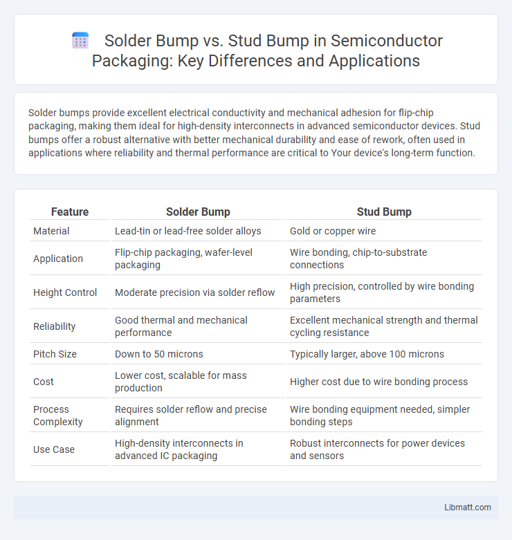
Table of Comparison
| Feature | Solder Bump | Stud Bump |
|---|---|---|
| Material | Lead-tin or lead-free solder alloys | Gold or copper wire |
| Application | Flip-chip packaging, wafer-level packaging | Wire bonding, chip-to-substrate connections |
| Height Control | Moderate precision via solder reflow | High precision, controlled by wire bonding parameters |
| Reliability | Good thermal and mechanical performance | Excellent mechanical strength and thermal cycling resistance |
| Pitch Size | Down to 50 microns | Typically larger, above 100 microns |
| Cost | Lower cost, scalable for mass production | Higher cost due to wire bonding process |
| Process Complexity | Requires solder reflow and precise alignment | Wire bonding equipment needed, simpler bonding steps |
| Use Case | High-density interconnects in advanced IC packaging | Robust interconnects for power devices and sensors |
Introduction to Solder Bump and Stud Bump Technologies
Solder bump technology involves depositing tiny balls of solder on semiconductor devices to establish electrical connections in flip-chip packaging, providing excellent mechanical strength and electrical conductivity. Stud bump technology uses wire bonding followed by deformation to create raised bumps, offering precise control over bump size and shape, beneficial for fine-pitch applications. Your choice between solder bump and stud bump technologies depends on factors like thermal performance, reliability, and manufacturing constraints.
Fundamental Differences: Solder Bump vs Stud Bump
Solder bumps consist of molten solder droplets used to create electrical interconnections in flip-chip packaging, enabling robust mechanical and electrical bonds with fine pitch capability. Stud bumps are formed by ball bonding techniques, typically using gold or copper wires, offering precise control in bump height and shape but limited by larger feature sizes. The fundamental difference lies in solder bumps relying on reflow processes for bonding, whereas stud bumps involve wire bonding and ultrasonic welding, impacting their applications in high-density microelectronics.
Materials Used in Solder and Stud Bumping
Solder bumping primarily uses tin-lead or lead-free solder alloys such as SnAgCu (tin-silver-copper) to create reliable electrical connections on semiconductor devices. Stud bumping typically involves gold or copper wire studs, formed through a ball bonding process and then flattened to create a bump on the substrate or die. The choice of materials affects mechanical strength, thermal conductivity, and compatibility with subsequent packaging processes.
Manufacturing Processes for Solder Bump and Stud Bump
Solder bump manufacturing involves depositing solder material onto wafer pads through electroplating, solder paste printing, or evaporation methods, followed by reflow to form uniform bumps. Stud bump fabrication uses a wire bonding process where a gold or copper wire is ultrasonically welded to the bond pad and then sheared to create the bump structure. Each method requires precise control of temperature, pressure, and alignment to ensure reliable interconnects in semiconductor packaging.
Electrical Performance Comparison
Solder bumps offer lower electrical resistance and better signal integrity due to their uniform shape and reliable metallurgical bonds, making them ideal for high-frequency applications. Stud bumps, while easier to fabricate and providing good mechanical strength, may introduce slightly higher resistance and parasitic inductance, impacting high-speed signal performance. Your choice depends on balancing electrical performance with manufacturing considerations and application-specific requirements.
Reliability and Durability Considerations
Solder bumps offer excellent electrical conductivity and thermal cycling reliability, making them suitable for high-performance semiconductor packaging. Stud bumps, created from solid metal, provide superior mechanical strength and durability under harsh environmental conditions, reducing the risk of mechanical failure in your devices. Choosing between solder bump vs stud bump depends on the specific reliability demands and durability requirements of your application.
Cost Implications: Solder Bump vs Stud Bump
Solder bumps generally offer lower initial manufacturing costs due to simpler deposition and reflow processes compared to stud bumps, which require more precise wire bonding and plating steps. However, stud bumps can reduce long-term expenses by minimizing failure rates and enhancing mechanical strength, leading to lower maintenance and replacement costs. The choice between solder and stud bumps ultimately depends on balancing upfront production budgets with reliability and performance requirements in semiconductor packaging.
Application Suitability in Modern Electronics
Solder bumps are widely used in high-density flip-chip packaging due to their excellent electrical conductivity and reliable mechanical bonding, making them ideal for applications requiring fine pitch interconnections such as advanced microprocessors and memory devices. Stud bumps, formed by wire bonding techniques, offer superior control over bump height and are preferred in applications demanding robust mechanical compliance and easier reworkability, especially in power electronics and sensors. Both technologies address different design and reliability requirements, with solder bumps favored for miniaturization and stud bumps for mechanical flexibility in modern electronic assemblies.
Challenges and Limitations of Each Technique
Solder bumps face challenges such as limited pitch scaling and susceptibility to void formation, which can degrade electrical performance and reliability. Stud bumps overcome some size constraints but encounter limitations in achieving uniform height and mechanical strength, impacting assembly yield. Your choice depends on balancing these factors with application-specific requirements for thermal and electrical conductivity.
Future Trends in Bump Technology
Future trends in bump technology emphasize enhanced electrical performance and miniaturization, with solder bumps advancing through the adoption of lead-free alloys and finer pitch capabilities. Stud bumps are gaining traction due to their superior mechanical strength and compatibility with advanced substrates like glass and silicon interposers. Integration of nano-materials and additive manufacturing techniques is expected to revolutionize both solder and stud bump formation, enabling higher reliability in next-generation semiconductor packaging.
Solder Bump vs Stud Bump Infographic