Mask sets are physical photomasks used in semiconductor manufacturing to transfer circuit patterns onto silicon wafers, while reticles refer specifically to the patterned glass plates used in photolithography equipment. Understanding the difference helps optimize your chip fabrication process by ensuring the right tool is selected for patterning accuracy and resolution.
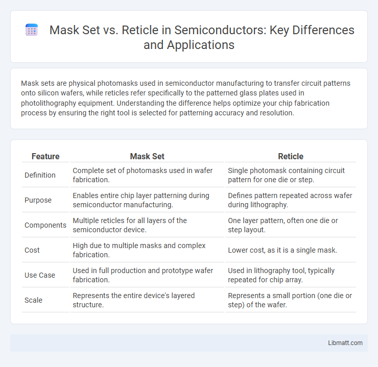
Table of Comparison
| Feature | Mask Set | Reticle |
|---|---|---|
| Definition | Complete set of photomasks used in wafer fabrication. | Single photomask containing circuit pattern for one die or step. |
| Purpose | Enables entire chip layer patterning during semiconductor manufacturing. | Defines pattern repeated across wafer during lithography. |
| Components | Multiple reticles for all layers of the semiconductor device. | One layer pattern, often one die or step layout. |
| Cost | High due to multiple masks and complex fabrication. | Lower cost, as it is a single mask. |
| Use Case | Used in full production and prototype wafer fabrication. | Used in lithography tool, typically repeated for chip array. |
| Scale | Represents the entire device's layered structure. | Represents a small portion (one die or step) of the wafer. |
Introduction to Mask Set and Reticle
A Mask Set is a collection of photomasks used in semiconductor manufacturing to pattern integrated circuits on silicon wafers, essential for defining device layers during lithography. A Reticle, often synonymous with a photomask, is a specific transparent plate with patterned features that project circuit designs onto wafers in photolithography tools. Understanding the distinction ensures you optimize your photolithography process by selecting the appropriate mask set and reticle for precise pattern transfer.
Definition and Core Functions
A Mask Set is a collection of photomasks used in semiconductor lithography to transfer circuit patterns onto wafers, essential for defining each layer of an integrated circuit during fabrication. A Reticle, also known as a photomask or mask plate, is a precise template containing the circuit pattern for a single layer, serving as the physical tool that projects the design onto the wafer through a photolithography system. Understanding the distinction between a Mask Set, which includes all reticles needed for a chip, and an individual Reticle helps optimize Your semiconductor manufacturing process by ensuring accurate pattern transfer and device functionality.
Key Differences Between Mask Set and Reticle
Mask set consists of multiple photomasks used in semiconductor manufacturing to define various layers, while a reticle is a single high-resolution photomask used specifically in photolithography steppers or scanners. Key differences include scope, as mask sets encompass the entire wafer patterning process, whereas reticles focus on one layer or pattern. Reticles are typically smaller and designed for repeated projection, while mask sets represent the complete layout for all layers of a chip.
Applications in Semiconductor Manufacturing
Mask sets and reticles are critical components in photolithography used for semiconductor manufacturing, where mask sets contain the full pattern for an entire wafer, and reticles typically hold patterns for individual die or chip layouts. Mask sets are essential for high-volume production, ensuring precise replication of complex circuit designs across multiple wafers, while reticles enable flexibility in testing and prototyping new semiconductor designs. Both tools contribute to improving yield, resolution, and alignment accuracy, which are vital for producing advanced microchips used in electronics, automotive, and telecommunications industries.
Advantages of Mask Set
Mask sets provide higher precision and consistency in semiconductor photolithography, enabling intricate patterning at nanometer scales. They allow rapid iteration during chip design cycles, reducing time-to-market for your integrated circuits. Enhanced durability and reusability of mask sets contribute to cost efficiency across large production volumes.
Benefits of Using Reticle
Reticles provide precise alignment and measurement capabilities that enhance the accuracy of photolithography processes compared to traditional mask sets. Using a reticle enables higher-resolution patterning and faster throughput due to its reduced size and compatibility with stepper systems. Your semiconductor fabrication benefits from reticle technology through improved yield and pattern fidelity, ultimately optimizing device performance and manufacturing efficiency.
Cost Implications and Scalability
Mask sets typically involve higher upfront costs due to the complex photomask fabrication process, making them less cost-effective for low-volume production runs. Reticles offer greater scalability and lower incremental expenses as they can be reused and adapted across various wafer sizes and production volumes. Your choice between mask set and reticle will significantly affect manufacturing expenses and long-term scalability strategies.
Impact on Lithography Process
The difference between a mask set and a reticle critically impacts the lithography process by determining resolution and pattern fidelity on semiconductor wafers. Mask sets comprise multiple photomasks for different layers, influencing throughput and alignment accuracy during photolithography. Your choice between the two affects pattern complexity and manufacturing precision, directly shaping device performance and yield.
Recent Innovations in Mask Set and Reticle Technology
Recent innovations in mask set and reticle technology have significantly enhanced photolithography precision for advanced semiconductor manufacturing at nodes below 5nm. Enhanced mask materials and pellicle designs improve defect control and yield by minimizing particle contamination during wafer exposure. Computational lithography advancements enable dynamic reticle pattern correction and high-resolution imaging, increasing manufacturing throughput and device performance.
Choosing Between Mask Set and Reticle: Key Considerations
Choosing between a mask set and a reticle requires evaluating factors such as design complexity, cost, and production volume. Mask sets offer flexibility for multiple device patterns and are suitable for initial prototyping, while reticles provide higher resolution and are essential for advanced photolithography in semiconductor fabrication. Consider the technology node requirements, throughput demands, and budget constraints to select the optimal option for integrated circuit manufacturing.
Mask Set vs Reticle Infographic