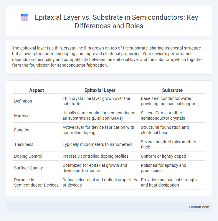
The epitaxial layer is a thin, crystalline film grown on top of the substrate, sharing its crystal structure but allowing for controlled doping and improved electrical properties. Your device's performance depends on the quality and compatibility between the epitaxial layer and the substrate, which together form the foundation for semiconductor fabrication.
Table of Comparison
| Aspect | Epitaxial Layer | Substrate |
|---|---|---|
| Definition | Thin crystalline layer grown over the substrate | Base semiconductor wafer providing mechanical support |
| Material | Usually same or similar semiconductor as substrate (e.g., silicon, GaAs) | Silicon, GaAs, or other semiconductor crystals |
| Function | Active layer for device fabrication with controlled doping | Structural foundation and electrical base |
| Thickness | Typically micrometers to nanometers | Several hundred micrometers thick |
| Doping Control | Precisely controlled doping profiles | Uniform or lightly doped |
| Surface Quality | Optimized for epitaxial growth and device performance | Polished for epitaxy and processing |
| Purpose in Semiconductor Devices | Defines electrical and optical properties of devices | Provides mechanical strength and heat dissipation |
Introduction to Epitaxial Layers and Substrates
Epitaxial layers are thin, crystalline films grown on a substrate that serve to improve the electronic properties of semiconductor devices by providing a controlled environment for charge carriers. Substrates act as the foundational base material, typically silicon or gallium arsenide, offering mechanical support as well as influencing the crystal orientation and quality of the epitaxial layer. Understanding the interaction between your substrate and epitaxial layer is crucial for optimizing semiconductor performance and device fabrication.
Defining Epitaxial Layer: Structure and Function
The epitaxial layer is a thin, crystallographically aligned layer grown on the substrate, typically silicon or another semiconductor material, serving as the foundation for device fabrication in microelectronics. Its structure ensures uniformity and minimal defects, enabling superior electrical properties compared to the underlying substrate, which acts as the mechanical support. Your device's performance heavily depends on the quality and characteristics of the epitaxial layer, influencing parameters like carrier mobility and junction depth.
Understanding Substrate Materials in Semiconductors
Substrate materials in semiconductors serve as the foundational layer upon which epitaxial layers are deposited, directly impacting device performance and manufacturing quality. Common substrates include silicon, gallium arsenide, and silicon carbide, each offering unique electrical and thermal properties tailored for specific applications. Understanding your substrate's crystalline structure, lattice constant, and thermal expansion coefficient is essential for optimizing epitaxial growth and ensuring the highest semiconductor device reliability.
Key Differences Between Epitaxial Layer and Substrate
The epitaxial layer is a thin, precisely controlled crystalline layer grown atop the substrate, which serves as the primary base material in semiconductor manufacturing. Unlike the substrate, which provides mechanical support and fundamental electrical properties, the epitaxial layer enables enhanced device performance through improved purity and tailored doping profiles. Your semiconductor devices rely on the epitaxial layer for optimized electronic characteristics, while the substrate ensures structural integrity and thermal management.
Role of Epitaxy in Semiconductor Device Fabrication
Epitaxy plays a crucial role in semiconductor device fabrication by enabling the growth of a high-quality epitaxial layer on a substrate, which serves as the foundation for device structures. The epitaxial layer provides precise control over doping concentration, thickness, and crystal orientation, resulting in improved electronic properties and device performance. Your semiconductor devices benefit from epitaxy through enhanced carrier mobility, reduced defects, and better junction control compared to the underlying substrate.
Growth Techniques for Epitaxial Layers
Epitaxial layers are typically grown on substrates using advanced techniques like Molecular Beam Epitaxy (MBE), Metal-Organic Chemical Vapor Deposition (MOCVD), and Liquid Phase Epitaxy (LPE). These methods enable precise control over layer thickness and composition, essential for semiconductor device performance. Understanding these growth techniques helps you optimize material quality and tailor the epitaxial layer properties to your specific application needs.
Material Compatibility: Epitaxial Layer vs Substrate
Material compatibility between the epitaxial layer and substrate is critical for achieving high-quality semiconductor devices, as lattice mismatch can lead to defects and dislocations. The epitaxial layer is grown on the substrate with closely matched crystal structures to ensure optimal electronic properties and minimal strain. You must select substrate materials that exhibit compatible thermal expansion coefficients and chemical properties with the epitaxial layer to prevent degradation during device fabrication.
Advantages of Using Epitaxial Layers
Epitaxial layers provide superior crystal quality and uniformity compared to substrates, enhancing electronic device performance and reliability. They enable precise control over doping concentrations and layer thickness, which is crucial for tailoring semiconductor properties to specific applications. Using epitaxial layers improves Your device efficiency and reduces defects, resulting in higher yields and better overall functionality.
Applications: Where Epitaxial Layers and Substrates Matter
Epitaxial layers are critical in semiconductor device fabrication, enabling high-performance applications such as integrated circuits, LEDs, and high-speed transistors due to their controlled crystal structure and purity. Substrates serve as the foundational base that provides mechanical support and influences electrical characteristics in devices like solar cells, microelectromechanical systems (MEMS), and power electronics. Your device's efficiency and reliability often depend on the precise interaction between the epitaxial layer and substrate materials tailored for specific technological applications.
Future Trends in Epitaxial Layer and Substrate Technologies
Future trends in epitaxial layer and substrate technologies emphasize the development of new materials such as gallium nitride (GaN) and silicon carbide (SiC) for high-power and high-frequency applications. Advancements in atomic layer deposition and molecular beam epitaxy techniques aim to enhance layer uniformity and reduce defect densities, boosting device performance and reliability. Integration of heterogeneous substrates supports the emergence of novel semiconductor devices, including those for 5G communications, electric vehicles, and advanced photonics.
Epitaxial Layer vs Substrate Infographic