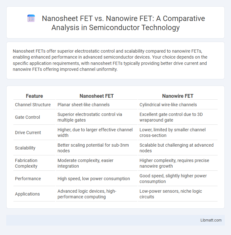
Nanosheet FETs offer superior electrostatic control and scalability compared to nanowire FETs, enabling enhanced performance in advanced semiconductor devices. Your choice depends on the specific application requirements, with nanosheet FETs typically providing better drive current and nanowire FETs offering improved channel uniformity.
Table of Comparison
| Feature | Nanosheet FET | Nanowire FET |
|---|---|---|
| Channel Structure | Planar sheet-like channels | Cylindrical wire-like channels |
| Gate Control | Superior electrostatic control via multiple gates | Excellent gate control due to 3D wraparound gate |
| Drive Current | Higher, due to larger effective channel width | Lower, limited by smaller channel cross-section |
| Scalability | Better scaling potential for sub-3nm nodes | Scalable but challenging at advanced nodes |
| Fabrication Complexity | Moderate complexity, easier integration | Higher complexity, requires precise nanowire growth |
| Performance | High speed, low power consumption | Good speed, slightly higher power consumption |
| Applications | Advanced logic devices, high-performance computing | Low-power sensors, niche logic circuits |
Introduction to Nanosheet FETs and Nanowire FETs
Nanosheet FETs and Nanowire FETs are advanced transistor architectures designed to enhance performance in nanoscale semiconductor devices. Nanosheet FETs utilize stacked, planar channels that provide improved electrostatic control and scalability compared to traditional FinFETs, while Nanowire FETs feature cylindrical channels offering excellent gate control and high on-off current ratios. Your choice between these technologies depends on specific application needs, with nanosheet FETs favoring higher drive current density and nanowire FETs excelling in minimizing leakage currents.
Device Structure Comparison
Nanosheet FETs feature a planar, stacked horizontal channel structure allowing larger effective channel width and enhanced electrostatic control, while nanowire FETs utilize a cylindrical channel with inherently better gate control due to the surround gate geometry. The multi-gate configuration in nanosheet FETs supports improved scalability and current drive capability compared to the point-contact characteristic of nanowire FETs. Fabrication of nanosheet FETs involves precise layer deposition and etching processes for the sheets, contrasting with nanowire FETs that require nanowire growth or etching techniques, impacting device complexity and variability.
Channel Control and Electrostatics
Nanosheet FETs offer superior channel control due to their wider planar geometry, enabling better electrostatic gate coupling and reduced short-channel effects compared to nanowire FETs. The 2D nanosheet structure provides enhanced scalability and stronger gate electrostatics by fully wrapping the channel, whereas nanowire FETs rely on cylindrical geometry with limited gate control around the channel circumference. Consequently, nanosheet FETs exhibit improved subthreshold slope, lower drain-induced barrier lowering (DIBL), and enhanced overall device performance in advanced semiconductor technologies.
Performance Metrics: Mobility and Conductance
Nanosheet FETs exhibit superior channel mobility compared to nanowire FETs due to their larger effective channel width and reduced surface scattering, enhancing carrier transport efficiency. Nanowire FETs offer higher electrostatic control but often suffer from lower conductance because of limited cross-sectional area and increased surface roughness scattering. Consequently, nanosheet FETs achieve improved drive current and overall conductance, making them advantageous for high-performance logic applications requiring enhanced mobility and conductance metrics.
Short Channel Effects in Nanosheet vs Nanowire FETs
Nanosheet FETs exhibit superior short channel effect (SCE) control compared to nanowire FETs due to their wider effective channel width and enhanced gate electrostatic control. The multi-gate architecture in nanosheet devices reduces drain-induced barrier lowering (DIBL) and subthreshold slope degradation more effectively than the cylindrical geometry of nanowire FETs. This leads to improved threshold voltage stability and lower leakage currents in nanosheet FETs, making them more scalable for advanced technology nodes.
Fabrication Challenges and Process Compatibility
Nanosheet FETs face fabrication challenges related to precise layer stacking and etching control to maintain uniform channel dimensions, demanding advanced lithography and deposition techniques. Nanowire FETs require intricate nanowire synthesis and alignment processes, making integration with existing CMOS workflows more complex. Process compatibility favors nanosheet FETs due to their planar structure, allowing easier adoption within standard semiconductor fabrication lines compared to the three-dimensional geometry of nanowire FETs.
Scalability for Advanced Technology Nodes
Nanosheet FETs exhibit superior scalability for advanced technology nodes due to their larger effective channel width and improved electrostatic control compared to Nanowire FETs, enabling continued transistor density scaling beyond 3nm. Nanowire FETs face challenges with variability and fabrication complexity as dimensions shrink, limiting their effectiveness at sub-5nm nodes. Your technology roadmap benefits from adopting Nanosheet FETs to achieve higher performance and power efficiency in future semiconductor processes.
Power Consumption and Efficiency
Nanosheet FETs demonstrate lower power consumption compared to Nanowire FETs due to their enhanced gate control and reduced short-channel effects, which improve subthreshold slope and reduce leakage currents. The planar geometry of Nanosheet FETs allows for better electrostatic control and higher drive current efficiency, resulting in improved overall device performance. In contrast, Nanowire FETs, while offering excellent gate electrostatics, tend to have higher parasitic capacitances that can increase power dissipation under high-frequency operation.
Applications in Modern Semiconductor Devices
Nanosheet FETs offer superior electrostatic control and scalability compared to Nanowire FETs, making them ideal for advanced logic circuits in modern semiconductor devices such as CPUs and GPUs. Nanowire FETs, with their excellent channel uniformity and high drive current, are suited for sensors and low-power applications in IoT devices. Your choice between these transistor types impacts device performance, power efficiency, and integration density in cutting-edge electronics.
Future Trends and Material Innovations
Nanosheet FETs are expected to dominate future semiconductor technology due to their superior scalability and enhanced electrostatic control compared to nanowire FETs, enabling higher performance in advanced nodes like 3nm and beyond. Material innovations such as integrating high-mobility channels using III-V compounds or 2D materials like transition metal dichalcogenides are driving the evolution of both nanosheet and nanowire devices. Your choice between these FET structures will depend on balancing trade-offs in fabrication complexity, drive current capabilities, and thermal performance as the industry moves towards heterogeneous integration and gate-all-around architectures.
Nanosheet FET vs Nanowire FET Infographic