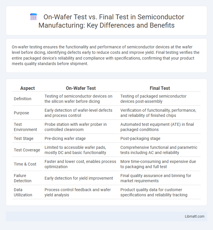
On-wafer testing ensures the functionality and performance of semiconductor devices at the wafer level before dicing, identifying defects early to reduce costs and improve yield. Final testing verifies the entire packaged device's reliability and compliance with specifications, confirming that your product meets quality standards before shipment.
Table of Comparison
| Aspect | On-Wafer Test | Final Test |
|---|---|---|
| Definition | Testing of semiconductor devices on the silicon wafer before dicing | Testing of packaged semiconductor devices post-assembly |
| Purpose | Early detection of wafer-level defects and process control | Verification of functionality, performance, and reliability of finished chips |
| Test Environment | Probe station with wafer prober in controlled cleanroom | Automated test equipment (ATE) in final packaged conditions |
| Test Stage | Pre-dicing wafer stage | Post-packaging stage |
| Test Coverage | Limited to accessible wafer pads, mostly DC and basic functionality | Comprehensive functional and parametric tests including AC and reliability |
| Time & Cost | Faster and lower cost, enables process optimization | More time-consuming and expensive due to packaging and full test |
| Failure Detection | Early detection for yield improvement | Final quality assurance and binning for market requirements |
| Data Utilization | Process control feedback and wafer yield analysis | Product quality data for customer specifications and reliability tracking |
Introduction to Semiconductor Testing
Semiconductor testing includes On-Wafer Test and Final Test, both essential for ensuring device functionality and yield. On-Wafer Test evaluates individual dies directly on the silicon wafer to detect early manufacturing defects and monitor process variations. Final Test verifies the fully packaged semiconductor device's performance and reliability before shipment, confirming compliance with industry specifications.
Defining On-Wafer Test
On-wafer test refers to the process of evaluating semiconductor devices directly on the silicon wafer before dicing and packaging, ensuring early detection of defects and performance verification. This method utilizes probe cards to access individual dies and measure electrical characteristics, enabling rapid feedback during wafer fabrication. On-wafer testing significantly reduces costs by identifying faulty dies early, improving yield management and overall semiconductor manufacturing efficiency.
Overview of Final Test
Final test validates the fully packaged semiconductor device, ensuring it meets all functional and performance specifications before shipment. This stage includes comprehensive stress tests, parametric measurements, and reliability assessments to detect latent defects not identifiable during on-wafer test. Accurate final test results are critical for quality assurance, customer satisfaction, and reducing field failures in electronic products.
Key Objectives of Each Testing Phase
On-wafer test aims to identify manufacturing defects and verify circuit functionality early in the production process, ensuring yield improvement and cost reduction. Final test focuses on validating overall device performance, reliability, and compliance with specifications after packaging to guarantee end-product quality and customer satisfaction. Your optimal testing strategy balances both phases to maximize defect detection and minimize production costs.
Equipment and Technology Used
On-wafer testing utilizes advanced probe stations equipped with high-precision micromanipulators and RF probes to evaluate semiconductor wafers directly at the wafer level, enabling early detection of defects before dicing. Final testing employs automated test equipment (ATE) systems designed for package-level evaluation, integrating high-throughput handlers and sophisticated electronic instrumentation to validate device functionality and performance under real-world conditions. Both testing phases rely on specialized technologies, but on-wafer tests focus on microscopic contact accuracy, while final tests prioritize speed and scalability for mass production validation.
Comparison of Test Parameters
On-wafer tests primarily focus on electrical parameters such as DC performance, leakage currents, and basic RF metrics at the wafer level before dicing, enabling early detection of fabrication defects. Final tests evaluate comprehensive parameters including full functional performance, timing, power consumption, and environmental stress at the packaged device stage, ensuring overall product reliability. Your choice between these tests hinges on balancing early defect identification with thorough validation of device operation post-packaging.
Cost and Time Implications
On-wafer testing significantly reduces overall production costs by identifying defects early in the semiconductor manufacturing process, minimizing waste and the need for expensive packaging of faulty chips. This testing method accelerates time-to-market since it enables rapid, high-throughput evaluation directly on the wafer before dicing, avoiding delays associated with post-packaging tests. Final testing, though more comprehensive, involves higher costs and longer time frames due to packaging and handling, making on-wafer test a cost-effective and time-efficient choice for early-stage quality control.
Typical Defects Detected
On-wafer testing primarily detects parametric defects such as open circuits, short circuits, and threshold voltage variations that occur during fabrication, allowing early identification of process-related issues. Final testing focuses on functional defects including incorrect logic operation, timing errors, and packaging-induced failures to ensure the semiconductor device performs correctly in real-world conditions. Your choice of testing strategy impacts defect detection efficiency and overall product quality assurance.
Impact on Yield and Quality
On-wafer testing enables early detection of defects during semiconductor fabrication, significantly improving yield by identifying faulty dies before packaging. Final testing, conducted post-packaging, ensures functional verification and reliability, directly influencing overall product quality. Combining both testing stages optimizes yield management and quality assurance in semiconductor manufacturing processes.
Choosing the Right Test Strategy
Choosing the right test strategy involves balancing the cost-effectiveness and accuracy between on-wafer test and final test methods. On-wafer testing offers early detection of defects directly on the semiconductor wafer, reducing wasted processing time and improving yield by screening out faulty dies before packaging. Your selection depends on factors like production volume, device complexity, and the criticality of performance parameters, ensuring efficient quality control throughout the manufacturing cycle.
On-Wafer Test vs Final Test Infographic