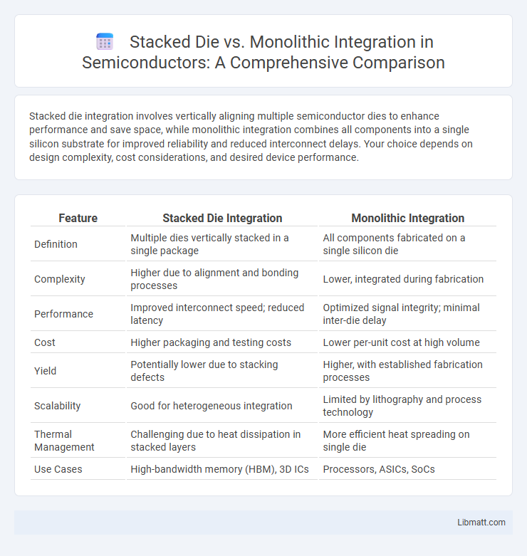
Stacked die integration involves vertically aligning multiple semiconductor dies to enhance performance and save space, while monolithic integration combines all components into a single silicon substrate for improved reliability and reduced interconnect delays. Your choice depends on design complexity, cost considerations, and desired device performance.
Table of Comparison
| Feature | Stacked Die Integration | Monolithic Integration |
|---|---|---|
| Definition | Multiple dies vertically stacked in a single package | All components fabricated on a single silicon die |
| Complexity | Higher due to alignment and bonding processes | Lower, integrated during fabrication |
| Performance | Improved interconnect speed; reduced latency | Optimized signal integrity; minimal inter-die delay |
| Cost | Higher packaging and testing costs | Lower per-unit cost at high volume |
| Yield | Potentially lower due to stacking defects | Higher, with established fabrication processes |
| Scalability | Good for heterogeneous integration | Limited by lithography and process technology |
| Thermal Management | Challenging due to heat dissipation in stacked layers | More efficient heat spreading on single die |
| Use Cases | High-bandwidth memory (HBM), 3D ICs | Processors, ASICs, SoCs |
Introduction to Stacked Die and Monolithic Integration
Stacked die integration involves vertically layering multiple semiconductor dies within a single package to enhance performance and reduce footprint, commonly used in 3D IC architectures. Monolithic integration fabricates multiple components on a single semiconductor substrate, enabling tighter interconnects and improved signal integrity for high-speed applications. Both approaches address scaling challenges in advanced electronics but differ in fabrication complexity and thermal management.
Defining Stacked Die Technology
Stacked die technology involves vertically layering multiple semiconductor dies within a single package to enhance performance and reduce footprint. This method improves interconnect density and bandwidth by shortening signal paths between dies, which is essential for advanced memory and processor applications. Compared to monolithic integration, which fabricates all components on a single silicon wafer, stacked die enables heterogeneous integration and greater design flexibility.
Understanding Monolithic Integration
Monolithic integration involves fabricating multiple electronic components or circuits within a single semiconductor substrate, enhancing signal integrity and reducing parasitic effects compared to stacked die architectures. This technique enables higher performance and lower power consumption by minimizing interconnect length and improving thermal management within a unified chip. Monolithic integration is widely used in applications requiring high-speed data processing and compact design, such as RF front-ends and advanced microprocessors.
Key Differences Between Stacked Die and Monolithic Integration
Stacked die integration involves vertically layering multiple semiconductor dies to enhance performance and reduce footprint, while monolithic integration fabricates all components on a single silicon substrate for improved signal integrity. Stacked die offers flexible heterogenous integration with potential thermal challenges, whereas monolithic integration ensures uniform material properties but limits design complexity. Your choice impacts device density, manufacturing cost, and system efficiency depending on application requirements.
Performance Advantages of Stacked Die
Stacked die integration enhances device performance by significantly reducing signal propagation delay and improving bandwidth through shorter interconnects compared to monolithic integration. This architecture enables higher transistor density and better thermal management, resulting in faster processing speeds and more efficient power consumption. Your systems benefit from increased scalability and the ability to integrate heterogeneous components, boosting overall performance beyond what monolithic designs typically achieve.
Benefits of Monolithic Integration
Monolithic integration enhances signal integrity by eliminating interconnect delays and reduces overall system size through the fabrication of multiple components on a single substrate. It improves power efficiency by minimizing parasitic capacitances and allows for better thermal management due to the compact and uniform structure. This integration approach also leads to cost savings in manufacturing by simplifying assembly and improving yield rates.
Applications and Use Cases
Stacked die integration excels in high-performance computing, memory modules, and multi-chip packaging due to its ability to combine heterogeneous technologies in a compact form factor, enhancing speed and bandwidth. Monolithic integration is preferred in applications requiring minimal latency and high reliability, such as RF circuits, sensors, and analog-digital mixed-signal devices, benefiting from a single substrate's uniformity. Your choice depends on whether your application prioritizes performance density or manufacturing simplicity and cost.
Design and Manufacturing Challenges
Stacked die integration faces significant challenges in heat dissipation and interconnect complexity due to vertical stacking, requiring advanced through-silicon vias (TSVs) and precise alignment for reliable performance. Monolithic integration simplifies interconnects by fabricating multiple layers on a single wafer, but it demands sophisticated process control to manage layer uniformity and defect minimization at the nanoscale. Both approaches require balancing cost, yield, and scalability while addressing unique thermal and mechanical stresses inherent to their design and manufacturing processes.
Cost Considerations and Scalability
Stacked die integration typically incurs higher initial manufacturing costs due to complex through-silicon via (TSV) technology and precision alignment requirements, but offers superior scalability by enabling increased transistor density and heterogeneous component stacking within a smaller footprint. Monolithic integration, while generally more cost-effective at volume because it uses standard fabrication processes without TSVs, may face scalability limitations due to wafer size constraints and heat dissipation challenges. Cost optimization in stacked die solutions improves over time with yield enhancements, making it suitable for high-performance applications demanding compact design and scalability beyond traditional monolithic approaches.
Future Trends in Semiconductor Integration
Future trends in semiconductor integration emphasize the shift toward stacked die technology, enabling higher performance and enhanced power efficiency through vertical scaling and heterogeneous integration. Monolithic integration continues to evolve with advances in process node miniaturization, delivering improved speed and lower latency for complex circuits. The convergence of these approaches supports next-generation applications such as AI acceleration, 5G networks, and advanced sensors, driving innovation in system-in-package (SiP) designs and 3D integrated circuits (3D ICs).
Stacked Die vs Monolithic Integration Infographic