Self-aligned gate technology in transistors allows precise alignment between the gate and source/drain regions, reducing parasitic capacitances and improving device performance compared to non-self-aligned gates. By using self-aligned gates, your circuits achieve higher speed and lower power consumption due to minimized overlap and enhanced control of channel formation.
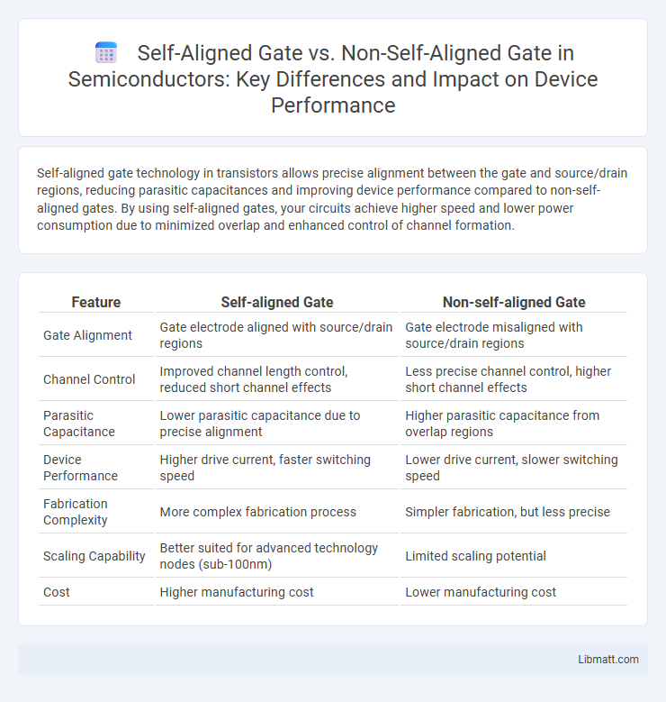
Table of Comparison
| Feature | Self-aligned Gate | Non-self-aligned Gate |
|---|---|---|
| Gate Alignment | Gate electrode aligned with source/drain regions | Gate electrode misaligned with source/drain regions |
| Channel Control | Improved channel length control, reduced short channel effects | Less precise channel control, higher short channel effects |
| Parasitic Capacitance | Lower parasitic capacitance due to precise alignment | Higher parasitic capacitance from overlap regions |
| Device Performance | Higher drive current, faster switching speed | Lower drive current, slower switching speed |
| Fabrication Complexity | More complex fabrication process | Simpler fabrication, but less precise |
| Scaling Capability | Better suited for advanced technology nodes (sub-100nm) | Limited scaling potential |
| Cost | Higher manufacturing cost | Lower manufacturing cost |
Introduction to Gate Technologies in Semiconductors
Self-aligned gate technology in semiconductors precisely aligns the gate electrode with the source and drain regions, minimizing parasitic capacitance and enhancing device performance. Non-self-aligned gates, in contrast, lack this precise alignment, leading to increased resistance and reduced efficiency in transistor operation. Your choice between these gate technologies significantly impacts the speed, power consumption, and scaling potential of integrated circuits.
What is a Self-Aligned Gate?
A Self-Aligned Gate (SAG) is a transistor gate fabrication technique where the gate electrode is precisely aligned with the source and drain regions, minimizing overlap and parasitic capacitance. This alignment improves device performance by reducing short-channel effects, enhancing drive current, and enabling more accurate channel formation. In contrast, Non-self-aligned gate processes have misaligned source/drain areas, leading to increased leakage and degraded transistor efficiency.
What is a Non-Self-Aligned Gate?
A Non-Self-Aligned Gate (NSAG) refers to a transistor gate structure where the gate electrode is not precisely aligned with the source and drain regions during fabrication, resulting in a larger overlap capacitance and increased parasitic resistance. Unlike self-aligned gates, NSAG devices require separate lithography steps for gate and source/drain patterning, which can lead to misalignment and reduced device performance. The non-self-aligned process typically results in slower switching speeds and higher power consumption in MOSFETs due to less optimal control over channel formation.
Structural Differences Between Self-Aligned and Non-Self-Aligned Gates
Self-aligned gates feature a fabrication process where the gate electrode precisely aligns with the source and drain regions, minimizing overlap and reducing parasitic capacitance for improved device performance. Non-self-aligned gates lack this precise alignment, leading to larger overlap areas between the gate and source/drain, which can increase leakage currents and degrade switching speeds. Your choice between these structures impacts transistor scaling and overall circuit efficiency due to their distinct structural differences.
Fabrication Process Comparison
The fabrication process of self-aligned gates involves using the gate electrode as a mask during source and drain implantation, ensuring precise alignment that reduces parasitic capacitance and short-channel effects. In contrast, non-self-aligned gate processes require separate patterning steps for the gate and source/drain regions, leading to misalignment issues and increased overlap capacitances. Your device performance benefits significantly from the reduced variability and improved electrical characteristics inherent in the self-aligned gate fabrication process.
Impact on Device Performance
Self-aligned gate technology significantly improves device performance by minimizing parasitic capacitance and reducing gate-to-source/drain overlap, leading to higher switching speeds and lower power consumption. Non-self-aligned gates typically exhibit increased leakage currents and reduced drive strength due to misaligned gate structures causing higher series resistance. Consequently, self-aligned gates enable enhanced device reliability and scalability in advanced semiconductor processes.
Advantages of Self-Aligned Gate Technology
Self-aligned gate technology offers superior device scalability and enhanced performance compared to non-self-aligned gates by precisely aligning the gate electrode with the source and drain regions, minimizing parasitic capacitance and resistance. This precise alignment reduces short-channel effects, improves drive current, and ensures better control over channel length, boosting overall transistor reliability and speed. Your integrated circuits benefit from improved power efficiency and increased packing density, critical for advanced semiconductor applications.
Drawbacks of Non-Self-Aligned Gate Structures
Non-self-aligned gate structures suffer from increased parasitic capacitance and resistance, leading to slower device switching speeds and higher power consumption. Misalignment between the gate and source/drain regions causes short-channel effects and degraded electrical performance, reducing overall device reliability. Your circuits benefit more from self-aligned gates due to their precision and improved scalability in advanced semiconductor technologies.
Applications and Industry Adoption
Self-aligned gate technology is widely adopted in advanced CMOS manufacturing due to its superior control over short-channel effects, making it essential for high-performance processors and memory devices in the semiconductor industry. Non-self-aligned gates are still utilized in niche applications like analog circuits and older fabrication nodes where simpler processes lower manufacturing costs. The preference for self-aligned gates continues to grow in industries focused on scaling down transistor dimensions, such as mobile electronics and automotive semiconductor sectors.
Future Trends in Gate Technology
Future trends in gate technology emphasize the advancement of self-aligned gate structures due to their superior electrical performance and scaling capabilities in nanoscale transistors. Non-self-aligned gates face challenges related to increased parasitic capacitance and variability, making self-aligned gates preferable for next-generation CMOS devices. Innovations such as high-k dielectric materials and metal gate electrodes are integrated predominantly with self-aligned processes to enhance device reliability and power efficiency.
Self-aligned Gate vs Non-self-aligned Gate Infographic