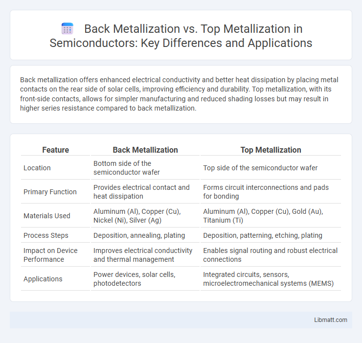
Back metallization offers enhanced electrical conductivity and better heat dissipation by placing metal contacts on the rear side of solar cells, improving efficiency and durability. Top metallization, with its front-side contacts, allows for simpler manufacturing and reduced shading losses but may result in higher series resistance compared to back metallization.
Table of Comparison
| Feature | Back Metallization | Top Metallization |
|---|---|---|
| Location | Bottom side of the semiconductor wafer | Top side of the semiconductor wafer |
| Primary Function | Provides electrical contact and heat dissipation | Forms circuit interconnections and pads for bonding |
| Materials Used | Aluminum (Al), Copper (Cu), Nickel (Ni), Silver (Ag) | Aluminum (Al), Copper (Cu), Gold (Au), Titanium (Ti) |
| Process Steps | Deposition, annealing, plating | Deposition, patterning, etching, plating |
| Impact on Device Performance | Improves electrical conductivity and thermal management | Enables signal routing and robust electrical connections |
| Applications | Power devices, solar cells, photodetectors | Integrated circuits, sensors, microelectromechanical systems (MEMS) |
Introduction to Metallization in Electronics
Metallization in electronics refers to the process of depositing metal layers on semiconductor devices to create electrical connections and interconnects. Back metallization involves applying metal contacts on the rear side of a wafer, enhancing heat dissipation and enabling better electrical performance in devices like solar cells and power semiconductors. Your choice between back and top metallization impacts device efficiency, cost, and manufacturing complexity, with top metallization typically used for front-side contacts due to its direct interface with active regions.
Defining Back Metallization and Top Metallization
Back metallization refers to the process of applying conductive metal layers on the rear side of a solar cell to form electrical contacts and facilitate current collection. Top metallization involves depositing fine metal grid lines on the front surface of the cell to collect sunlight-generated charges while minimizing shading losses. Understanding these metallization techniques is crucial for optimizing Your solar cell efficiency and manufacturing processes.
Materials Used in Back and Top Metallization
Back metallization commonly utilizes aluminum due to its excellent conductivity and good adhesion to silicon, often supplemented with zinc or silver to enhance mechanical strength and electrical performance. Top metallization typically employs materials such as silver or silver alloys because of their superior conductivity and reflectivity, which improve solar cell efficiency by reducing resistive losses and maximizing light capture. Both methods incorporate layers like titanium or nickel as adhesion or barrier layers, optimizing the metallization's durability and electrical contact quality.
Process Differences: Back vs Top Metallization
Back metallization involves applying conductive material on the rear side of a semiconductor wafer, enhancing electrical contact and heat dissipation, while top metallization places metals on the wafer's front surface for direct connection to circuits. The back metallization process requires backside cleaning, deposition, and annealing to ensure low resistance and strong adhesion, whereas top metallization focuses on photolithography, patterning, and multiple metal layer depositions to create intricate circuit pathways. Understanding these process differences can help optimize your device's performance and manufacturing efficiency based on application-specific requirements.
Electrical Performance Comparison
Back metallization offers superior electrical performance by reducing the series resistance and enhancing current collection efficiency, which is crucial for high-efficiency solar cells. Top metallization can cause shading and increase contact resistance, negatively impacting power output. Your choice between back and top metallization directly affects the electrical conductivity and overall energy conversion efficiency of photovoltaic devices.
Impact on Device Efficiency and Reliability
Back metallization enhances device efficiency by improving electrical contact and reducing shading on the active surface, leading to better light absorption and charge collection. Top metallization, while easier to apply and inspect, can cause increased shading and higher series resistance, potentially lowering overall efficiency. In terms of reliability, back metallization offers superior protection against environmental degradation, resulting in longer device lifespan and stability under thermal and mechanical stress.
Manufacturing Challenges and Solutions
Back metallization offers improved heat dissipation but poses manufacturing challenges such as precise alignment and higher costs due to complex processing steps. Top metallization simplifies contact formation but can cause shading losses and requires careful optimization of metal layout to enhance efficiency. Your choice between these methods depends on balancing production efficiency with performance needs through advanced techniques like laser patterning and selective plating.
Applications and Use Cases
Back metallization is commonly used in solar cells to improve electrical contact and maximize light absorption, making it ideal for high-efficiency photovoltaic panels. Top metallization is crucial in semiconductor devices for creating precise circuit patterns and enhancing signal transmission in integrated circuits. Your choice between back and top metallization depends on specific application requirements such as device architecture, electrical performance, and manufacturing constraints.
Cost Implications and Scalability
Back metallization offers lower production costs due to simpler fabrication processes and reduced material usage, making it advantageous for large-scale manufacturing. Top metallization, while often providing better electrical performance and contact precision, involves more complex, costly lithography steps that can hinder scalability. Choosing back metallization can result in significant cost savings and enhanced scalability for high-volume semiconductor applications.
Future Trends in Metallization Technologies
Back metallization and top metallization technologies are evolving rapidly, driven by the demand for higher efficiency and cost-effective solar cells. Emerging trends include advanced materials like silver-aluminum alloys and copper plating for improved conductivity and reduced material costs. You can expect future metallization techniques to integrate nano-structured patterns and hybrid methods, enhancing electrical performance while minimizing shading losses.
Back Metallization vs Top Metallization Infographic