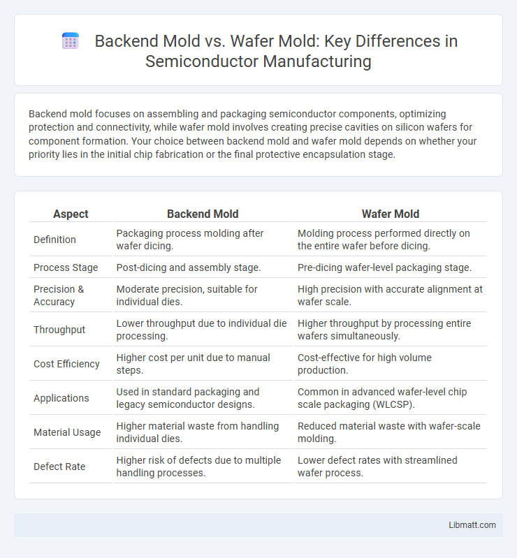
Backend mold focuses on assembling and packaging semiconductor components, optimizing protection and connectivity, while wafer mold involves creating precise cavities on silicon wafers for component formation. Your choice between backend mold and wafer mold depends on whether your priority lies in the initial chip fabrication or the final protective encapsulation stage.
Table of Comparison
| Aspect | Backend Mold | Wafer Mold |
|---|---|---|
| Definition | Packaging process molding after wafer dicing. | Molding process performed directly on the entire wafer before dicing. |
| Process Stage | Post-dicing and assembly stage. | Pre-dicing wafer-level packaging stage. |
| Precision & Accuracy | Moderate precision, suitable for individual dies. | High precision with accurate alignment at wafer scale. |
| Throughput | Lower throughput due to individual die processing. | Higher throughput by processing entire wafers simultaneously. |
| Cost Efficiency | Higher cost per unit due to manual steps. | Cost-effective for high volume production. |
| Applications | Used in standard packaging and legacy semiconductor designs. | Common in advanced wafer-level chip scale packaging (WLCSP). |
| Material Usage | Higher material waste from handling individual dies. | Reduced material waste with wafer-scale molding. |
| Defect Rate | Higher risk of defects due to multiple handling processes. | Lower defect rates with streamlined wafer process. |
Introduction to Backend Mold and Wafer Mold
Backend mold refers to the specialized tooling used in the semiconductor packaging process to shape and encapsulate integrated circuits during chip assembly. Wafer mold, on the other hand, involves molds designed for wafer-level packaging, allowing for simultaneous processing of multiple chips directly on the wafer surface. These two mold types play critical roles in enhancing semiconductor device reliability and performance through precise microfabrication methods.
Key Differences Between Backend and Wafer Mold
Backend molds focus on final packaging and assembly of semiconductor devices, shaping and encapsulating chips, while wafer molds are used during the initial wafer fabrication to create micro-scale circuit patterns on silicon wafers. Wafer molds require extreme precision and cleanroom conditions to ensure defect-free circuitry, whereas backend molds prioritize durability and thermal management for completed chip assemblies. Understanding these key differences helps you optimize manufacturing workflows based on device complexity and production stage.
Overview of Backend Mold Technology
Backend mold technology in semiconductor manufacturing involves creating precise molds used for encapsulating and protecting integrated circuits after wafer fabrication. Unlike wafer molds, which shape the silicon wafer during front-end processing, backend molds focus on packaging elements such as transfer molding, compression molding, and encapsulation for improved thermal management and mechanical protection. Advanced backend mold techniques enhance device reliability and performance by optimizing mold compound properties and minimizing warpage and residual stress.
Detailed Explanation of Wafer Mold Process
The wafer mold process involves placing multiple semiconductor devices onto a single silicon wafer to create uniform imprints using photolithography and etching techniques. This method enhances production efficiency by enabling simultaneous molding of numerous components, ensuring consistent micro-scale pattern accuracy and reducing manufacturing defects. Wafer molds are crucial in high-volume semiconductor fabrication, delivering precise, repeatable results for integrated circuit packaging.
Applications of Backend Mold in Semiconductor Manufacturing
Backend mold is crucial in semiconductor manufacturing for packaging and protecting integrated circuits, ensuring electrical connections are precisely encapsulated to maintain device performance and reliability. It is widely applied in flip-chip and wafer-level packaging processes, catering to high-volume production of consumer electronics, automotive sensors, and communication devices. Your understanding of backend mold applications can optimize the manufacturing workflow and improve final product durability.
Wafer Mold: Use Cases and Industry Adoption
Wafer molds are extensively used in semiconductor manufacturing for producing microelectronic devices with high precision and scalability, especially in integrated circuit fabrication. Their adoption is prominent in industries like consumer electronics, automotive sensors, and telecommunications due to their ability to handle complex, miniaturized designs efficiently. Wafer molds enable mass production with consistent quality, supporting advancements in MEMS devices and high-density integrated chips.
Material Selection for Backend and Wafer Mold
Material selection for backend molds typically involves metals like copper alloys and aluminum due to their excellent thermal conductivity and mechanical strength, ensuring durability during packaging processes. Wafer molds often use high-purity silicon or quartz materials to maintain precision and minimize contamination at the microscopic level crucial for semiconductor fabrication. Your choice depends on balancing cost, thermal performance, and compatibility with the specific manufacturing stage.
Advantages and Limitations: Backend Mold vs Wafer Mold
Backend molds offer enhanced customization for specific packaging requirements, improving chip performance and reliability through tailored encapsulation processes, but they may increase production complexity and cost. Wafer molds enable high-throughput and uniform encapsulation at the wafer level, leading to consistent quality and scalability, though they can limit individual device optimization and flexibility. Balancing backend mold precision with wafer mold efficiency depends on the application's demand for customization versus mass production economics.
Future Trends in Mold Technologies for Semiconductors
Future trends in semiconductor mold technologies emphasize increased precision and miniaturization, with wafer mold approaches gaining traction due to their scalability and cost efficiency in mass production. Backend molds focus on improving thermal management and electrical performance through advanced materials and integrated designs, enhancing overall device reliability. Your choice between backend and wafer mold technologies should consider evolving demands for higher integration, reduced footprint, and faster manufacturing cycles in semiconductor applications.
Choosing the Right Mold Process for Your Application
Selecting the right mold process between backend mold and wafer mold depends on the specific application requirements such as package size, complexity, and production volume. Backend molds are preferred for larger packages requiring higher mechanical strength and efficient heat dissipation, while wafer molds excel in high-precision applications with smaller footprints and higher integration levels. Understanding factors like thermal management, cost-effectiveness, and throughput ensures optimal performance and reliability in semiconductor packaging.
Backend Mold vs Wafer Mold Infographic