Planar transistors feature a flat channel design that allows current to flow horizontally, but they face limitations in controlling leakage and scaling as device dimensions shrink. FinFETs use a 3D fin-like structure to improve gate control over the channel, reducing power consumption and enhancing performance, which makes them ideal for your advanced, high-density semiconductor applications.
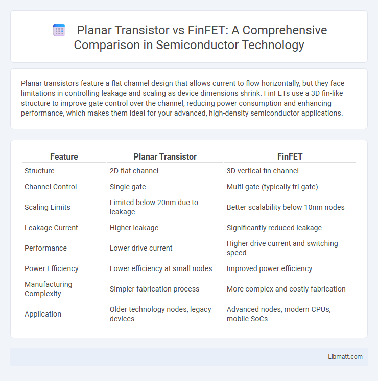
Table of Comparison
| Feature | Planar Transistor | FinFET |
|---|---|---|
| Structure | 2D flat channel | 3D vertical fin channel |
| Channel Control | Single gate | Multi-gate (typically tri-gate) |
| Scaling Limits | Limited below 20nm due to leakage | Better scalability below 10nm nodes |
| Leakage Current | Higher leakage | Significantly reduced leakage |
| Performance | Lower drive current | Higher drive current and switching speed |
| Power Efficiency | Lower efficiency at small nodes | Improved power efficiency |
| Manufacturing Complexity | Simpler fabrication process | More complex and costly fabrication |
| Application | Older technology nodes, legacy devices | Advanced nodes, modern CPUs, mobile SoCs |
Introduction to Planar Transistor and FinFET
Planar transistors, traditional components in semiconductor devices, feature a flat channel through which current flows, making them simpler to manufacture but less efficient at controlling short-channel effects in advanced nodes. FinFETs, or Fin Field-Effect Transistors, utilize a 3D fin-like structure to wrap the gate around the channel, significantly enhancing electrostatic control and performance at smaller scales. Understanding these differences helps you choose the right technology for optimizing power efficiency and scaling in modern integrated circuits.
Historical Evolution of Transistor Technologies
The historical evolution of transistor technologies highlights the transition from planar transistors to FinFETs as a response to scaling limitations and performance demands in semiconductor devices. Planar transistors dominated the industry for decades, utilizing a flat channel structure suitable for early integrated circuits but facing short-channel effects as feature sizes shrank below 45nm. FinFET technology emerged around the mid-2000s with a 3D fin-shaped channel that provides better electrostatic control, reduced leakage currents, and enhanced drive current, enabling continued Moore's Law scaling and powering modern high-performance processors and mobile devices.
Structural Differences: Planar vs. FinFET
Planar transistors feature a flat, two-dimensional channel where current flows horizontally between the source and drain, controlled by a gate on top. In contrast, FinFETs utilize a three-dimensional fin-shaped channel that protrudes vertically from the substrate, allowing the gate to wrap around multiple sides of the fin, enhancing electrostatic control. This 3D structure significantly reduces short-channel effects and improves performance in nanoscale semiconductor devices.
Performance Comparison: Speed and Efficiency
FinFET technology offers superior speed and efficiency compared to planar transistors due to its three-dimensional structure, which provides better control over channel electrostatics and substantially reduces short-channel effects. The enhanced gate control in FinFETs leads to lower leakage current and higher drive current, significantly improving switching speed and power efficiency. As a result, FinFETs outperform planar transistors in high-performance and low-power applications, making them the preferred choice for advanced semiconductor manufacturing processes below 16nm technology nodes.
Power Consumption and Leakage Current
FinFET transistors significantly reduce power consumption and leakage current compared to planar transistors due to their 3D structure, which provides better electrostatic control over the channel. The improved gate control in FinFETs minimizes off-state leakage current, enhancing energy efficiency and performance in your devices. This makes FinFET technology a preferred choice for low-power and high-performance applications.
Scalability and Miniaturization Limitations
Planar transistors face significant scalability challenges as channel lengths approach the 5-nanometer node, leading to short-channel effects and increased leakage currents that hinder further miniaturization. FinFET technology, with its three-dimensional gate structure, offers superior control over the channel, enabling efficient operation at smaller nodes and improved electrostatic integrity. Your choice between planar and FinFET impacts device performance and power efficiency, especially as semiconductor fabrication pushes beyond traditional scaling limits.
Manufacturing Complexity and Cost
Planar transistors feature simpler manufacturing processes due to their established 2D structure, resulting in lower fabrication costs compared to FinFETs. FinFET technology introduces a 3D gate structure that significantly increases manufacturing complexity, requiring advanced lithography and etching techniques. This complexity leads to higher production costs but enables improved performance and power efficiency, making FinFETs more suitable for cutting-edge semiconductor nodes.
Impact on Device Reliability and Longevity
Planar transistors suffer from increased leakage currents and short-channel effects that can degrade device reliability over time, while FinFETs offer improved electrostatic control and reduced leakage, significantly enhancing longevity. FinFET's three-dimensional structure enables better gate control, lowering power consumption and heat generation that contribute to device wear-out mechanisms. As a result, FinFET technology is more resilient under high-performance and high-temperature conditions, extending the operational life of semiconductor devices.
Industry Adoption and Future Trends
FinFET technology has rapidly overtaken planar transistors in industry adoption due to its superior performance, reduced leakage current, and enhanced scalability at sub-20nm nodes. Leading semiconductor companies like Intel, TSMC, and Samsung have transitioned to FinFETs for advanced process nodes, optimizing power efficiency and switching speeds in modern CPUs and GPUs. Your designing efforts in next-gen electronics will likely benefit from FinFET's continued innovation, with emerging trends pointing toward gate-all-around (GAA) transistors as the future evolution beyond FinFET architectures.
Conclusion: Choosing Between Planar and FinFET
Planar transistors offer simpler manufacturing and are cost-effective for mature technology nodes above 22nm, while FinFETs provide superior performance, power efficiency, and scalability at advanced nodes below 22nm due to their 3D structure. FinFETs reduce leakage current and improve electrostatic control, making them ideal for high-performance and low-power applications in modern semiconductor designs. Selecting between planar and FinFET depends on the target process node, performance requirements, and cost constraints of the device.
Planar Transistor vs FinFET Infographic