Through Glass Via (TGV) offers superior electrical insulation and optical transparency, making it ideal for high-frequency microelectronics and optoelectronics, whereas Through Silicon Via (TSV) provides higher thermal conductivity and mechanical strength, suitable for 3D integrated circuits and advanced semiconductor packaging. Your choice depends on whether you prioritize insulation and transparency with TGV or robust thermal performance and integration density with TSV.
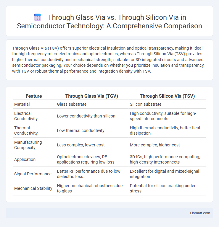
Table of Comparison
| Feature | Through Glass Via (TGV) | Through Silicon Via (TSV) |
|---|---|---|
| Material | Glass substrate | Silicon substrate |
| Electrical Conductivity | Lower conductivity than silicon | High conductivity, suitable for high-speed interconnects |
| Thermal Conductivity | Low thermal conductivity | High thermal conductivity, better heat dissipation |
| Manufacturing Complexity | Less complex, lower cost | More complex, higher cost |
| Application | Optoelectronic devices, RF applications requiring low loss | 3D ICs, high-performance computing, high-density interconnects |
| Signal Performance | Better RF performance due to low dielectric loss | Excellent for digital and mixed-signal integration |
| Mechanical Stability | Higher mechanical robustness due to glass | Potential for silicon cracking under stress |
Introduction to Through Glass Via (TGV) and Through Silicon Via (TSV)
Through Glass Via (TGV) and Through Silicon Via (TSV) are advanced interconnect technologies used in 3D integrated circuits to enhance chip performance and miniaturization. TGV involves creating vertical electrical connections through glass substrates, offering advantages like low dielectric constant and high-frequency signal integrity, while TSV refers to vertical vias etched through silicon wafers, enabling efficient heat dissipation and high-density interconnects. Both technologies play critical roles in heterogeneous integration, with TGV favored in RF applications and TSV predominant in microelectronics and 3D stacking.
Technological Overview: TGV vs TSV
Through Glass Via (TGV) and Through Silicon Via (TSV) are advanced 3D interconnect technologies enabling vertical electrical connections in microelectronics. TGV uses glass substrates offering high insulation, low parasitic capacitance, and excellent signal integrity, making it suitable for RF and photonic applications. TSV involves drilling vertical holes in silicon wafers and filling them with conductive material, providing superior thermal conductivity and high-density interconnects essential for high-performance computing and memory integration.
Material Properties: Glass versus Silicon
Glass offers excellent electrical insulation and low dielectric constant, reducing signal loss and crosstalk in through glass vias (TGVs). Silicon, used in through silicon vias (TSVs), provides superior thermal conductivity and mechanical strength, supporting efficient heat dissipation and structural integrity in 3D integrated circuits. The choice between glass and silicon materials impacts device performance, thermal management, and manufacturing complexity.
Fabrication Processes for TGV and TSV
Through Glass Via (TGV) fabrication involves laser drilling or wet etching to create vias in glass substrates, followed by metallization to form conductive pathways, enabling high-frequency signal transmission with low loss. Through Silicon Via (TSV) fabrication employs deep reactive ion etching (DRIE) to form vertical channels in silicon wafers, subsequently insulated and filled with copper or tungsten to achieve high-density 3D integration in semiconductor devices. Both processes require precise alignment and planarization techniques, but TGV offers advantages in RF applications due to the low dielectric constant and excellent insulating properties of glass compared to silicon.
Electrical Performance Comparison
Through Glass Via (TGV) offers superior electrical performance compared to Through Silicon Via (TSV) due to its lower dielectric constant and reduced parasitic capacitance, resulting in lower signal loss and crosstalk. TGV structures exhibit lower resistance and improved signal integrity, making them ideal for high-frequency applications and RF modules. Your choice between TGV and TSV will significantly impact device speed, power consumption, and overall efficiency in advanced semiconductor packaging.
Thermal Management in TGV and TSV
Through Glass Via (TGV) offers superior thermal insulation compared to Through Silicon Via (TSV), reducing heat dissipation challenges in densely packed 3D integrated circuits. TSV, made from silicon, provides better thermal conductivity, facilitating efficient heat transfer but potentially causing hotspots without adequate cooling solutions. Optimizing thermal management in TGV and TSV involves balancing insulation and conductivity to prevent thermal stress and ensure device reliability in advanced semiconductor packaging.
Reliability and Mechanical Strength
Through Silicon Via (TSV) offers superior mechanical strength compared to Through Glass Via (TGV) due to silicon's inherent toughness and compatibility with semiconductor processes. TGV's reliability is often challenged by glass fragility and thermal mismatch, potentially leading to microcracks under stress or thermal cycling. Advanced bonding techniques and optimized via filling materials improve TGV reliability, but TSV remains the preferred choice for high-performance, mechanically robust 3D integrated circuits.
Cost and Scalability Factors
Through Glass Via (TGV) offers lower material costs due to the use of glass substrates, which are less expensive than silicon. Scalability in TGV is enhanced by simpler manufacturing processes and reduced etching complexity compared to Through Silicon Via (TSV), improving throughput for high-volume production. TSV incurs higher costs stemming from silicon wafer expenses and complex deep reactive ion etching, which can limit scalability in mass production environments.
Applications and Use Cases
Through Glass Via (TGV) technology is predominantly used in advanced optical and RF applications due to its excellent electrical insulation and high-frequency performance, making it ideal for photonic devices, 5G antennas, and sensors. Through Silicon Via (TSV) is widely adopted in 3D integrated circuits and memory stacking technologies to enable high-density, high-speed interconnects in processors, DRAM, and image sensors. TGV's compatibility with transparent substrates supports applications in display technologies and microelectromechanical systems (MEMS), while TSV's robustness suits large-scale semiconductor packaging and heterogeneous integration in high-performance computing.
Future Trends: TGV and TSV in Advanced Packaging
Through Glass Via (TGV) and Through Silicon Via (TSV) technologies are pivotal in the evolution of advanced packaging, offering enhanced electrical performance and miniaturization for 3D integrated circuits. Future trends indicate increasing integration of TGV for high-frequency applications due to its excellent dielectric properties and thermal stability, while TSV continues to dominate in heterogeneous integration involving silicon-based components. The convergence of TGV and TSV is expected to drive innovation in high-density interposers and system-in-package (SiP) solutions, enabling faster data transmission and improved power efficiency in next-generation electronic devices.
Through Glass Via vs Through Silicon Via Infographic