Planarization ensures a flat surface by removing topographical variations, while Chemical Mechanical Planarization (CMP) combines chemical etching and mechanical polishing for precise, smooth wafer surfaces. Your semiconductor manufacturing process benefits significantly from CMP's ability to achieve global surface planarity crucial for advanced device fabrication.
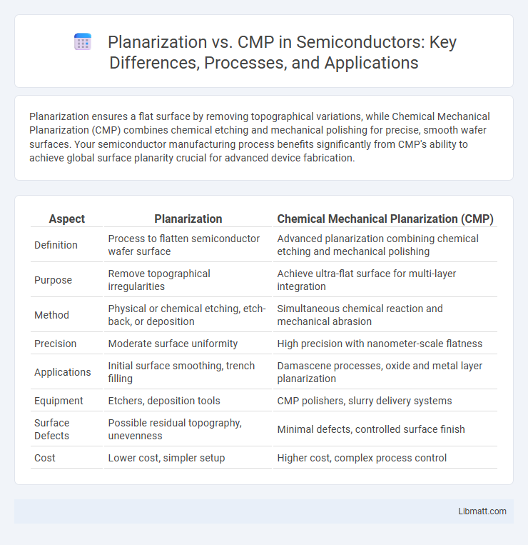
Table of Comparison
| Aspect | Planarization | Chemical Mechanical Planarization (CMP) |
|---|---|---|
| Definition | Process to flatten semiconductor wafer surface | Advanced planarization combining chemical etching and mechanical polishing |
| Purpose | Remove topographical irregularities | Achieve ultra-flat surface for multi-layer integration |
| Method | Physical or chemical etching, etch-back, or deposition | Simultaneous chemical reaction and mechanical abrasion |
| Precision | Moderate surface uniformity | High precision with nanometer-scale flatness |
| Applications | Initial surface smoothing, trench filling | Damascene processes, oxide and metal layer planarization |
| Equipment | Etchers, deposition tools | CMP polishers, slurry delivery systems |
| Surface Defects | Possible residual topography, unevenness | Minimal defects, controlled surface finish |
| Cost | Lower cost, simpler setup | Higher cost, complex process control |
Introduction to Planarization and CMP
Planarization is a critical semiconductor fabrication process used to create a flat and uniform surface on a wafer, essential for subsequent photolithography steps. Chemical Mechanical Planarization (CMP) is a specialized planarization technique combining chemical etching and mechanical polishing to achieve precise surface leveling with high control over topography. Your chip manufacturing success depends on choosing the appropriate planarization method to meet specific device requirements and enhance performance.
Defining Planarization in Semiconductor Manufacturing
Planarization in semiconductor manufacturing refers to the process of making a wafer surface flat and even to ensure precise layering during chip fabrication. Chemical Mechanical Polishing (CMP) is a widely used planarization technique that combines chemical slurry and mechanical abrasion to achieve a uniform surface topology. Your ability to select the most effective planarization method directly impacts device performance, yield, and overall manufacturing quality.
What is Chemical Mechanical Planarization (CMP)?
Chemical Mechanical Planarization (CMP) is a critical semiconductor fabrication process combining chemical etching and mechanical polishing to achieve an ultra-flat wafer surface. It removes topographical variations caused by prior deposition and patterning, enabling precise photolithography and layer stacking in integrated circuits. Your chip's performance and yield depend heavily on the uniformity and smoothness produced by CMP compared to traditional planarization methods.
Key Differences: Planarization vs CMP
Planarization is a general process that smooths surfaces in semiconductor manufacturing, while Chemical Mechanical Planarization (CMP) is a specific technique combining chemical and mechanical forces to achieve ultra-flat wafer surfaces. CMP offers superior precision in removing topography variations compared to traditional planarization methods, making it essential for advanced integrated circuit fabrication. Your semiconductor production benefits from CMP's ability to provide uniform layer thickness and reduced defects, critical for device performance and yield.
Importance of Surface Flatness in Microfabrication
Surface flatness is crucial in microfabrication to ensure precise pattern transfer and uniform layer deposition. Planarization techniques, including Chemical Mechanical Planarization (CMP), enhance wafer surface uniformity by removing topographical variations, which directly impacts device performance and yield. Your microfabrication process benefits from CMP's ability to achieve nanoscale flatness necessary for advanced semiconductor device manufacturing.
Techniques Used for Planarization
Planarization techniques are essential for creating a flat surface in semiconductor manufacturing, with Chemical Mechanical Planarization (CMP) being the most widely used method. CMP combines chemical etching and mechanical polishing to achieve high precision and uniformity across the wafer, effectively removing topographical variations. Your choice between planarization methods depends on factors such as film type, desired surface roughness, and process integration requirements.
Advantages and Limitations of CMP
Chemical Mechanical Planarization (CMP) offers superior global surface planarization critical for advanced semiconductor manufacturing, enabling increased device density and improved photolithography accuracy. CMP effectively removes topographical variations and defects but requires precise process control to avoid issues such as dishing, erosion, and slurry contamination. Limitations include high operational costs and difficulties in handling diverse materials, necessitating thorough optimization for consistent wafer surface quality.
Applications of Planarization and CMP in Industry
Planarization and Chemical Mechanical Polishing (CMP) are critical in semiconductor manufacturing for creating flat surfaces essential in photolithography and multilayer device fabrication. CMP is widely applied in the production of integrated circuits, where it removes excess material to achieve global and local planarity, improving device performance and yield. Planarization techniques are also utilized in microelectromechanical systems (MEMS), optical devices, and advanced packaging to ensure surface uniformity and enhance component reliability.
Challenges in Achieving Optimal Planarity
Achieving optimal planarity in planarization processes faces significant challenges such as non-uniform material removal rates and topography variation across wafers. Chemical Mechanical Polishing (CMP) must precisely balance mechanical abrasion and chemical etching to prevent defects like dishing and erosion. Controlling process parameters like slurry composition, pad condition, and pressure distribution is critical to overcoming these planarization challenges and ensuring uniform surface flatness.
Future Trends in Planarization and CMP Technologies
Future trends in planarization and Chemical Mechanical Planarization (CMP) technologies emphasize the integration of advanced metrology and real-time process control to enhance uniformity and reduce defects in semiconductor manufacturing. Emerging techniques focus on eco-friendly slurry formulations and novel abrasive particles to minimize environmental impact while improving efficiency. The development of AI-driven predictive models is accelerating process optimization, ensuring better wafer surface quality and supporting the demands of next-generation microelectronics.
Planarization vs CMP Infographic