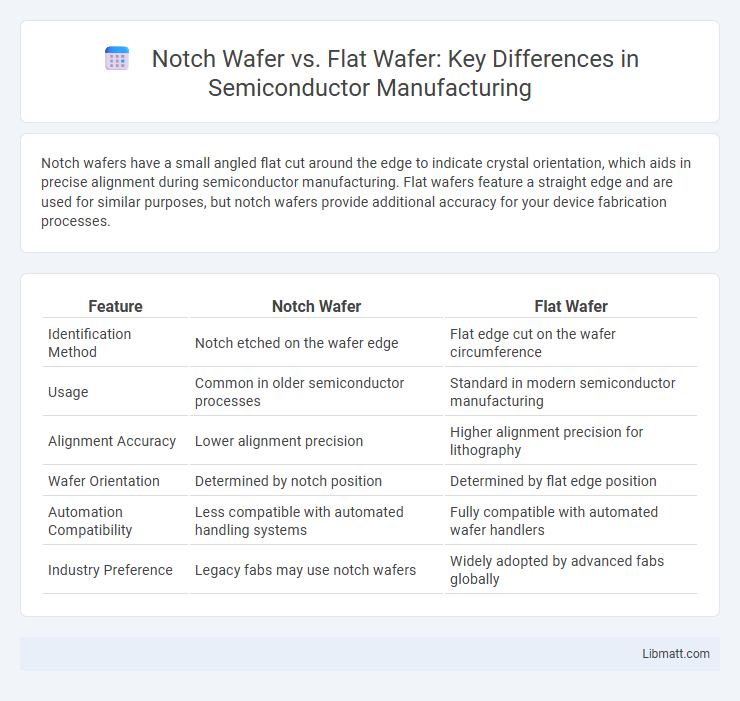
Notch wafers have a small angled flat cut around the edge to indicate crystal orientation, which aids in precise alignment during semiconductor manufacturing. Flat wafers feature a straight edge and are used for similar purposes, but notch wafers provide additional accuracy for your device fabrication processes.
Table of Comparison
| Feature | Notch Wafer | Flat Wafer |
|---|---|---|
| Identification Method | Notch etched on the wafer edge | Flat edge cut on the wafer circumference |
| Usage | Common in older semiconductor processes | Standard in modern semiconductor manufacturing |
| Alignment Accuracy | Lower alignment precision | Higher alignment precision for lithography |
| Wafer Orientation | Determined by notch position | Determined by flat edge position |
| Automation Compatibility | Less compatible with automated handling systems | Fully compatible with automated wafer handlers |
| Industry Preference | Legacy fabs may use notch wafers | Widely adopted by advanced fabs globally |
Introduction to Notch Wafer and Flat Wafer
Notch wafers and flat wafers are two types of silicon wafers used in semiconductor manufacturing, distinguished by their edge markings that indicate crystal orientation. Notch wafers feature a small, precise notch on the edge, aiding automated equipment in identifying wafer alignment and orientation for processing. Flat wafers, on the other hand, use a flat edge as a reference, providing a simpler but equally effective way to determine crystal direction and ensure accurate device fabrication on your semiconductor devices.
Overview of Semiconductor Wafer Types
Notch wafers and flat wafers are common semiconductor wafer types distinguished by their edge markings, which assist in crystal orientation during device fabrication. Notch wafers feature a small indentation used to identify specific crystallographic planes, while flat wafers include one or more flat edges serving the same purpose for alignment and processing consistency. Understanding the differences between these wafer types is essential for optimizing Your semiconductor manufacturing workflow and ensuring precise device performance.
What is a Notch Wafer?
A Notch Wafer is a type of semiconductor wafer characterized by a small, precisely cut indentation on its edge, which serves as a physical alignment mark during manufacturing. This notch helps equipment and technicians identify the wafer's crystal orientation, ensuring accurate layer deposition and patterning in integrated circuit fabrication. Compared to Flat Wafers, which use a flat edge instead of a notch for orientation, Notch Wafers allow for higher precision in wafer handling and processing steps.
What is a Flat Wafer?
A flat wafer is a silicon substrate used in semiconductor manufacturing characterized by one or more flats--precisely cut edges--that serve as orientation marks for crystal alignment during device fabrication. These flats enable accurate positioning of photolithographic masks to ensure consistent doping, etching, and layering processes. Compared to notch wafers, flat wafers provide a simpler shape recognition method crucial for maintaining uniformity in integrated circuit production.
Key Differences Between Notch and Flat Wafers
Notch wafers feature a small indentation on the edge to indicate crystal orientation, crucial for aligning wafers during semiconductor manufacturing, while flat wafers use a flat edge or edges to serve the same purpose. The notch provides precise directional reference, aiding in consistent device performance and process control, whereas flat wafers may facilitate easier handling but with less orientation precision. Understanding whether your process requires notch or flat wafers directly affects alignment accuracy and overall fabrication quality.
Advantages of Notch Wafers
Notch wafers offer precise orientation identification, which enhances alignment accuracy during semiconductor fabrication processes. This leads to improved wafer handling and reduces the risk of errors in photolithography and etching, contributing to higher yield and device performance. Your manufacturing workflow benefits from the consistent orientation provided by notch wafers, enabling efficient and reliable production.
Advantages of Flat Wafers
Flat wafers offer improved alignment accuracy during semiconductor manufacturing, reducing defects and enhancing yield rates. Their consistent edge geometry simplifies handling and automation processes in wafer fabrication plants. Additionally, flat wafers enable more precise photolithography, contributing to higher device performance and reliability.
Applications in the Semiconductor Industry
Notch wafers are widely used in semiconductor manufacturing for precise crystal orientation identification during device fabrication, ensuring accurate photolithography alignment. Flat wafers, while also serving orientation purposes, are favored in applications requiring simpler wafer handling and inspection processes. Your choice between notch and flat wafers depends on the specific requirements of semiconductor devices, such as microprocessors or memory chips, where wafer orientation impacts yield and performance.
Choosing Between Notch and Flat Wafers
Choosing between notch wafer and flat wafer depends on your specific semiconductor manufacturing needs, as notch wafers feature an angled cut that serves as an orientation marker, while flat wafers have a straight edge used similarly but with different industry standards. Notch wafers are often preferred for high-precision alignment and compatibility with advanced lithography equipment, whereas flat wafers are commonly used in simpler processes requiring basic orientation. Your selection influences the wafer handling, alignment accuracy, and compatibility with equipment, impacting overall production efficiency and yield.
Future Trends in Wafer Technology
Future trends in wafer technology emphasize the transition from traditional flat wafers to notch wafers for enhanced alignment precision in semiconductor manufacturing. Notch wafers provide superior orientation control, crucial for advanced lithography and yield improvement in emerging nodes like 3nm and beyond. Your production processes will benefit from wafer designs that support high-volume manufacturing with greater defect detection and reduced variability.
Notch Wafer vs Flat Wafer Infographic