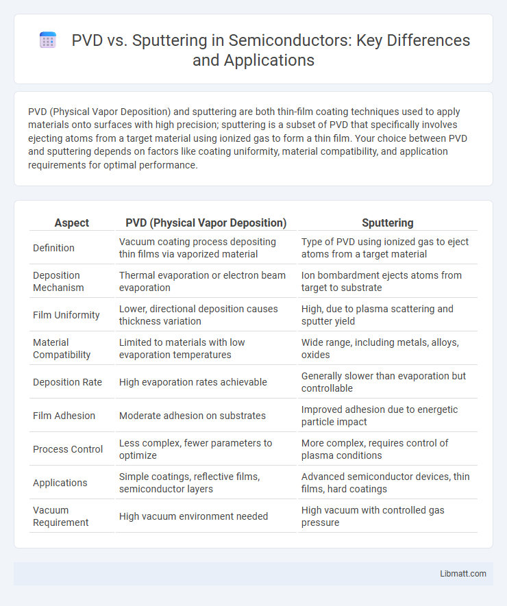
PVD (Physical Vapor Deposition) and sputtering are both thin-film coating techniques used to apply materials onto surfaces with high precision; sputtering is a subset of PVD that specifically involves ejecting atoms from a target material using ionized gas to form a thin film. Your choice between PVD and sputtering depends on factors like coating uniformity, material compatibility, and application requirements for optimal performance.
Table of Comparison
| Aspect | PVD (Physical Vapor Deposition) | Sputtering |
|---|---|---|
| Definition | Vacuum coating process depositing thin films via vaporized material | Type of PVD using ionized gas to eject atoms from a target material |
| Deposition Mechanism | Thermal evaporation or electron beam evaporation | Ion bombardment ejects atoms from target to substrate |
| Film Uniformity | Lower, directional deposition causes thickness variation | High, due to plasma scattering and sputter yield |
| Material Compatibility | Limited to materials with low evaporation temperatures | Wide range, including metals, alloys, oxides |
| Deposition Rate | High evaporation rates achievable | Generally slower than evaporation but controllable |
| Film Adhesion | Moderate adhesion on substrates | Improved adhesion due to energetic particle impact |
| Process Control | Less complex, fewer parameters to optimize | More complex, requires control of plasma conditions |
| Applications | Simple coatings, reflective films, semiconductor layers | Advanced semiconductor devices, thin films, hard coatings |
| Vacuum Requirement | High vacuum environment needed | High vacuum with controlled gas pressure |
Introduction to PVD and Sputtering
Physical Vapor Deposition (PVD) involves the transfer of material from a source to a substrate through vaporized particles, creating thin films with high adhesion and precision. Sputtering, a common PVD technique, utilizes ionized gas to eject atoms from a target material which then deposit onto the substrate, offering excellent coating uniformity and control. Your choice between PVD and sputtering depends on material compatibility, coating requirements, and desired film properties.
Understanding Physical Vapor Deposition (PVD)
Physical Vapor Deposition (PVD) is a vacuum coating process that involves vaporizing solid materials into a plasma state and depositing them as thin films onto substrates, ensuring high purity and strong adhesion. Compared to sputtering, PVD techniques such as evaporation provide precise control over film thickness and composition, making it suitable for applications requiring uniform and dense coatings. Understanding the differences in material interaction and energy transfer helps optimize your surface engineering projects for enhanced corrosion resistance and wear protection.
What is Sputtering?
Sputtering is a physical vapor deposition (PVD) technique where atoms are ejected from a solid target material due to bombardment by energetic ions, typically from a plasma source. This process deposits a thin, uniform film of the target material onto a substrate, enabling precise coating control in semiconductor manufacturing and optical applications. Understanding sputtering helps you optimize thin film properties for enhanced device performance.
Key Differences Between PVD and Sputtering
Physical Vapor Deposition (PVD) and sputtering are both thin film deposition techniques used in various industries, but they differ fundamentally in their processes. PVD encompasses a range of methods including evaporation and sputtering, where material is vaporized from a solid source to form a thin film, while sputtering specifically involves ejecting material from a target by bombarding it with high-energy ions. Understanding these key differences helps you select the appropriate technique based on factors like film adhesion, uniformity, and the types of materials involved in your application.
Applications of PVD Technology
Physical Vapor Deposition (PVD) technology is widely used in various industries, including semiconductor manufacturing, aerospace, and automotive sectors, for coating tools, decorative finishes, and wear-resistant surfaces. PVD enables precise control over film thickness and composition, making it essential for producing microelectronics, optical coatings, and cutting tools with enhanced durability. Your choice of PVD can improve product performance by delivering high-quality, uniform coatings tailored to specific application requirements.
Sputtering in Industrial Processes
Sputtering in industrial processes is a highly controlled physical vapor deposition (PVD) technique used to deposit thin films with uniform thickness and excellent adhesion on various substrates. This method offers precise control over film composition, making it ideal for semiconductor manufacturing, coating of optical devices, and production of hard, wear-resistant surfaces. Your production efficiency and product quality significantly benefit from sputtering's ability to create dense, defect-free coatings with tailored properties.
Advantages and Disadvantages of PVD
Physical Vapor Deposition (PVD) offers advantages such as excellent coating adhesion, high precision in thin film thickness control, and the ability to deposit a wide range of materials on various substrates. However, PVD typically requires a high vacuum environment, which can increase operational costs and limit the size of the substrates you can coat. Its lower deposition rates compared to sputtering may also affect production speed in large-scale manufacturing.
Pros and Cons of Sputtering
Sputtering offers excellent film uniformity and strong adhesion, making it ideal for coating complex shapes and producing thin films with precise thickness control. However, it tends to have lower deposition rates and higher equipment costs compared to Physical Vapor Deposition (PVD), which can increase production time and expenses. If your application demands high-quality, uniform coatings on intricate components, sputtering provides superior performance despite these trade-offs.
Choosing Between PVD and Sputtering
Choosing between Physical Vapor Deposition (PVD) and sputtering depends on your specific coating requirements, as PVD offers high deposition rates and excellent adhesion for decorative or protective films, while sputtering provides superior control over film thickness and uniformity, ideal for complex and precise applications. Sputtering allows better coverage of intricate surfaces and a wider range of target materials, making it suitable for semiconductor and optical industries. You should evaluate factors like substrate type, desired film properties, and production scale to select the optimal technique for your coating needs.
Future Trends in Surface Coating Technologies
Future trends in surface coating technologies emphasize enhanced precision and energy efficiency in PVD (Physical Vapor Deposition) and sputtering processes, driven by advancements in atomic-level control and sustainable materials. Innovations in magnetron sputtering improve deposition rates and uniformity, while emerging hybrid PVD-sputtering systems aim to optimize coating properties for aerospace and semiconductor industries. Your choice between PVD and sputtering will increasingly depend on the demand for ultra-thin, high-performance coatings with minimal environmental impact.
PVD vs Sputtering Infographic