Epitaxy involves the precise growth of a crystalline layer on a substrate, ensuring atomic alignment for high-quality semiconductor devices, while implantation introduces ions into the substrate to modify electrical properties without altering the crystal structure. Your choice between epitaxy and implantation impacts the performance and reliability of semiconductor components in advanced electronics.
Table of Comparison
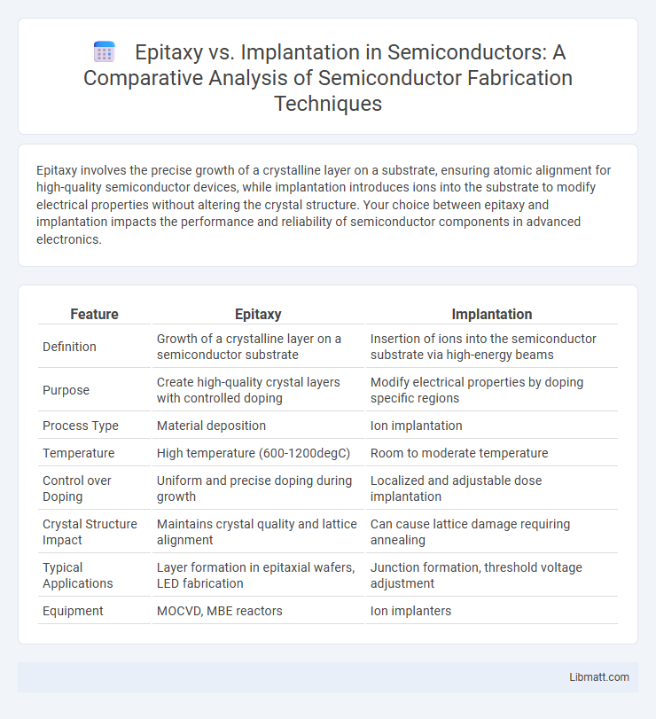
| Feature | Epitaxy | Implantation |
|---|---|---|
| Definition | Growth of a crystalline layer on a semiconductor substrate | Insertion of ions into the semiconductor substrate via high-energy beams |
| Purpose | Create high-quality crystal layers with controlled doping | Modify electrical properties by doping specific regions |
| Process Type | Material deposition | Ion implantation |
| Temperature | High temperature (600-1200degC) | Room to moderate temperature |
| Control over Doping | Uniform and precise doping during growth | Localized and adjustable dose implantation |
| Crystal Structure Impact | Maintains crystal quality and lattice alignment | Can cause lattice damage requiring annealing |
| Typical Applications | Layer formation in epitaxial wafers, LED fabrication | Junction formation, threshold voltage adjustment |
| Equipment | MOCVD, MBE reactors | Ion implanters |
Introduction to Epitaxy and Implantation
Epitaxy involves the precise growth of a crystalline layer on a substrate, maintaining the crystal structure to enhance semiconductor device performance. Implantation refers to the process of injecting ions into a semiconductor to modify its electrical properties by altering the material's doping profile. Your choice between epitaxy and implantation depends on the specific requirements for layer thickness, doping control, and device architecture in semiconductor manufacturing.
Defining Epitaxy: Fundamentals and Techniques
Epitaxy involves the growth of a crystalline layer on a substrate crystal, maintaining the same lattice structure to ensure high-quality semiconductor materials essential for advanced electronic devices. Techniques such as Molecular Beam Epitaxy (MBE) and Metal-Organic Chemical Vapor Deposition (MOCVD) enable precise control over layer thickness, composition, and doping, crucial for optimizing device performance. Understanding these fundamentals allows you to select epitaxy methods tailored to specific semiconductor applications, differentiating it from implantation, which introduces dopants by ion bombardment rather than crystal growth.
Understanding Ion Implantation in Semiconductors
Ion implantation involves accelerating ions into a semiconductor substrate to precisely alter its electrical properties by introducing dopants at controlled depths and concentrations. This technique enables accurate modification of conductivity without disrupting the crystal lattice structure, unlike epitaxy, which grows new crystalline layers on the substrate surface. Understanding ion implantation helps optimize semiconductor device performance by enabling tailored doping profiles critical for modern integrated circuits.
Epitaxy vs Implantation: Key Differences
Epitaxy involves the growth of a crystalline layer on a substrate, maintaining crystal alignment, while implantation is the process of introducing dopant ions into the substrate through ion bombardment. Epitaxy offers high-quality, defect-free layers essential for semiconductor device performance, whereas implantation provides precise control over dopant concentration and depth. The choice between epitaxy and implantation depends on specific device requirements such as layer uniformity, electrical properties, and manufacturing complexity.
Material Quality: Epitaxial Layers vs Implanted Regions
Epitaxial layers provide superior material quality with highly crystalline, defect-free structures essential for high-performance semiconductor devices. In contrast, implanted regions often suffer from crystal damage and defects that require annealing to partially restore material integrity. Your choice between epitaxy and implantation impacts device reliability and electronic properties due to these inherent differences in material quality.
Process Advantages and Limitations
Epitaxy offers precise control over crystal quality and thickness, enabling the growth of defect-free silicon layers critical for high-performance semiconductor devices, while its limitation includes high equipment costs and complex process conditions. Ion implantation provides accurate dopant placement with excellent dose and depth control, allowing for scalable and repeatable doping across wafers, but it can cause crystal damage requiring subsequent annealing to restore material properties. Both processes are essential in semiconductor fabrication, with epitaxy favoring structural perfection and implantation optimizing electrical characteristics.
Applications in Semiconductor Device Fabrication
Epitaxy enables the growth of high-quality crystalline semiconductor layers with precise control over thickness and doping, crucial for fabricating advanced transistors, LEDs, and laser diodes. Ion implantation allows for precise doping of semiconductor substrates by embedding ions at controlled depths, essential for forming pn-junctions in integrated circuits and modifying electrical properties without affecting crystal integrity. Combining epitaxy and implantation techniques optimizes device performance, enabling complex multilayer structures and tailored electrical characteristics in modern semiconductor manufacturing.
Cost and Efficiency Considerations
Epitaxy offers higher device performance through superior crystal quality but involves more complex, expensive equipment and longer processing times, impacting cost efficiency. Ion implantation provides greater control over dopant profiles with relatively lower capital expenses and faster throughput, making it more cost-effective for large-scale production. Your choice depends on balancing the need for precise material properties with budget constraints and manufacturing speed.
Future Trends in Epitaxy and Implantation
Future trends in epitaxy focus on atomic-layer precision and the integration of novel materials like III-V semiconductors and 2D materials to enhance device performance and energy efficiency. Implantation advancements emphasize ultra-low energy ion beams and advanced annealing techniques that improve doping profiles and minimize lattice damage for next-generation nanoelectronics. Both epitaxy and implantation are evolving with AI-driven process controls and in-situ monitoring to achieve higher yield and scalability in semiconductor manufacturing.
Conclusion: Choosing the Right Process
Choosing between epitaxy and implantation depends on your semiconductor device requirements, as epitaxy offers superior crystal quality and precise layer control for high-performance applications, while implantation provides flexibility in doping profiles and is cost-effective for mass production. Consider epitaxy when device efficiency and uniformity are critical, and opt for implantation if process adaptability and lower costs are prioritized. Understanding these differences ensures your fabrication process aligns with the desired electrical and structural characteristics of your device.
Epitaxy vs Implantation Infographic