Wafer bumping enhances semiconductor device connectivity by adding tiny metal bumps on the wafer surface, improving electrical performance and enabling advanced packaging. Wafer thinning reduces the wafer's thickness to improve heat dissipation and enable flexible, lightweight designs, complementing your device's miniaturization and thermal management needs.
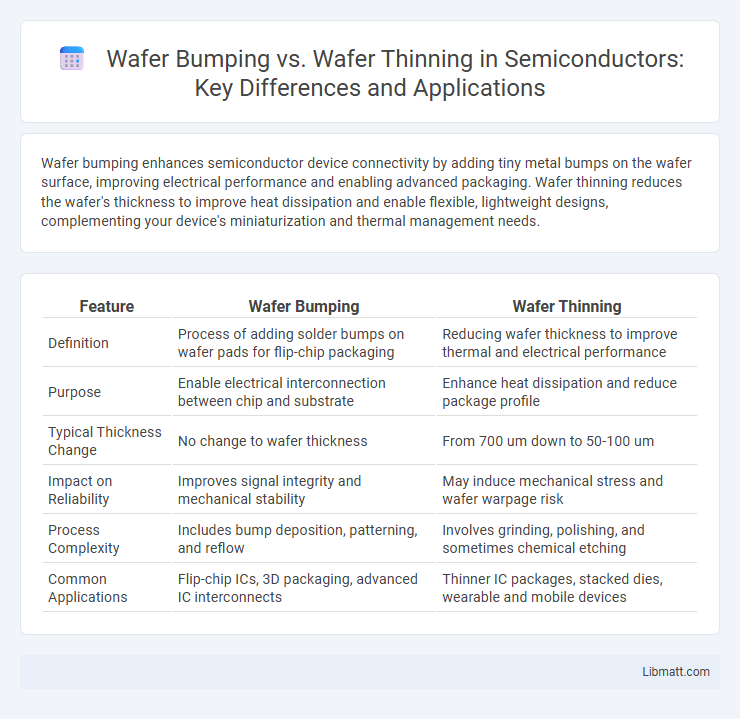
Table of Comparison
| Feature | Wafer Bumping | Wafer Thinning |
|---|---|---|
| Definition | Process of adding solder bumps on wafer pads for flip-chip packaging | Reducing wafer thickness to improve thermal and electrical performance |
| Purpose | Enable electrical interconnection between chip and substrate | Enhance heat dissipation and reduce package profile |
| Typical Thickness Change | No change to wafer thickness | From 700 um down to 50-100 um |
| Impact on Reliability | Improves signal integrity and mechanical stability | May induce mechanical stress and wafer warpage risk |
| Process Complexity | Includes bump deposition, patterning, and reflow | Involves grinding, polishing, and sometimes chemical etching |
| Common Applications | Flip-chip ICs, 3D packaging, advanced IC interconnects | Thinner IC packages, stacked dies, wearable and mobile devices |
Introduction to Wafer Bumping and Wafer Thinning
Wafer bumping involves depositing small solder bumps on a semiconductor wafer to enable electrical connections in flip-chip packaging, enhancing signal transmission and thermal performance. Wafer thinning reduces the thickness of a wafer to improve heat dissipation and enable miniaturization of electronic devices. Your choice between wafer bumping and wafer thinning depends on the specific requirements for device integration and performance optimization.
Key Differences Between Wafer Bumping and Wafer Thinning
Wafer bumping involves adding tiny solder bumps to the wafer surface to enable electrical connections in advanced packaging, while wafer thinning reduces the wafer's thickness to improve heat dissipation and enable flexible or miniaturized devices. The key difference lies in their purposes: wafer bumping primarily enhances interconnectivity through surface modification, whereas wafer thinning targets mechanical and thermal performance by decreasing substrate thickness. Your choice depends on whether connectivity optimization or physical wafer integrity is the priority in semiconductor manufacturing.
Importance of Wafer Bumping in Semiconductor Packaging
Wafer bumping plays a crucial role in advanced semiconductor packaging by creating electrical and mechanical connections between the silicon die and the substrate, enabling higher input/output density and improved signal integrity. It supports the implementation of 3D integration and system-in-package (SiP) technologies, which are essential for miniaturization and enhanced device performance. Compared to wafer thinning, which primarily reduces die thickness for better thermal management and form factor, wafer bumping directly influences interconnect reliability and overall package robustness in modern microelectronics.
Role of Wafer Thinning in Advanced IC Manufacturing
Wafer thinning plays a critical role in advanced IC manufacturing by reducing the wafer thickness to enhance heat dissipation and improve electrical performance, enabling higher device density and reliability. This process facilitates better stacking and integration in 3D ICs, complementing wafer bumping, which provides precise electrical interconnections through solder bumps. Together, wafer thinning and wafer bumping enable the production of compact, high-performance semiconductor packages essential for modern electronics.
Wafer Bumping Process Steps Explained
Wafer bumping involves depositing microscopic solder bumps on a wafer's surface to enable electrical connections in advanced semiconductor packaging. The process steps include wafer cleaning, under bump metallurgy (UBM) deposition, solder paste application, reflow soldering to form bumps, and inspection for quality assurance. Understanding each stage ensures your semiconductor devices achieve reliable performance and high-density interconnects.
Wafer Thinning Process Steps and Techniques
Wafer thinning involves reducing the thickness of semiconductor wafers through precise grinding, polishing, and etching processes to enhance device performance and integration. Common techniques include mechanical grinding to remove bulk material, chemical mechanical polishing (CMP) for surface planarization, and wet or dry etching to achieve ultra-thin measurements with minimal damage. These controlled steps improve thermal management and enable advanced packaging solutions such as 3D ICs and wafer-level chip scale packaging (WLCSP).
Advantages of Wafer Bumping Technology
Wafer bumping technology offers significant advantages such as improved electrical performance and mechanical stability by providing short interconnect lengths and enhancing signal integrity. It enables higher input/output density, facilitating advanced packaging solutions like flip-chip bonding, which is essential for miniaturized, high-performance semiconductor devices. Your designs benefit from better thermal management and increased reliability, making wafer bumping a preferred choice over wafer thinning in many high-speed, high-density applications.
Benefits of Wafer Thinning for Modern Devices
Wafer thinning enhances modern device performance by significantly reducing device thickness, leading to improved heat dissipation and enabling ultra-compact form factors essential for wearable and mobile technologies. It also facilitates better electrical performance through shorter interconnect lengths and supports advanced packaging techniques like 3D IC integration. These benefits contribute to increased device reliability, enhanced signal integrity, and lower power consumption critical for next-generation electronics.
Challenges in Wafer Bumping vs Wafer Thinning
Challenges in wafer bumping include precise control of solder ball placement and alignment to ensure reliable electrical connections, while managing thermal stresses that can lead to defects during reflow. In wafer thinning, maintaining wafer integrity and preventing breakage or warpage pose significant difficulties, alongside achieving uniform thickness without compromising device performance. Your selection between these processes depends on balancing the mechanical robustness and electrical reliability required for advanced semiconductor packaging.
Future Trends in Wafer Bumping and Thinning Technologies
Future trends in wafer bumping emphasize the integration of finer pitch bumps and the adoption of lead-free solder materials to enhance electrical performance and environmental compliance. Wafer thinning technology advances focus on ultrathin wafers below 50 microns, improving device flexibility and enabling next-generation 3D integration and heterogeneous packaging. Both wafer bumping and thinning are converging towards achieving higher density interconnects, improved thermal management, and compatibility with emerging semiconductor nodes like 3nm and beyond.
Wafer Bumping vs Wafer Thinning Infographic