Plasma dicing offers a precise, crack-free method for separating semiconductor wafers using reactive ion etching, minimizing mechanical stress and damage compared to traditional mechanical dicing which employs saw blades that can induce micro-cracks and particle contamination. Choosing plasma dicing can enhance your device yield and reliability by ensuring cleaner edges and reducing chipping associated with mechanical processes.
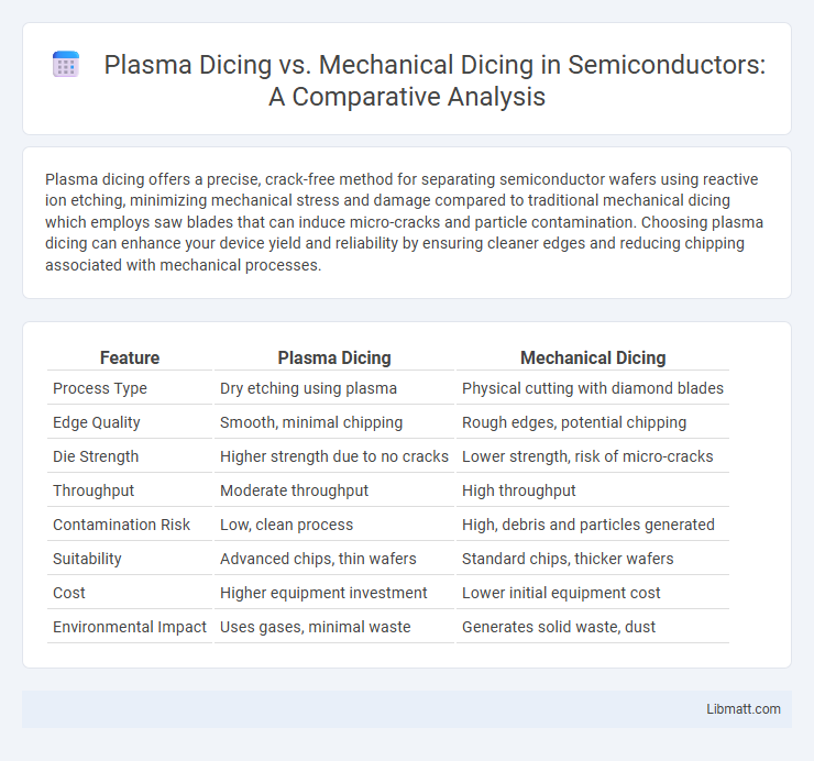
Table of Comparison
| Feature | Plasma Dicing | Mechanical Dicing |
|---|---|---|
| Process Type | Dry etching using plasma | Physical cutting with diamond blades |
| Edge Quality | Smooth, minimal chipping | Rough edges, potential chipping |
| Die Strength | Higher strength due to no cracks | Lower strength, risk of micro-cracks |
| Throughput | Moderate throughput | High throughput |
| Contamination Risk | Low, clean process | High, debris and particles generated |
| Suitability | Advanced chips, thin wafers | Standard chips, thicker wafers |
| Cost | Higher equipment investment | Lower initial equipment cost |
| Environmental Impact | Uses gases, minimal waste | Generates solid waste, dust |
Introduction to Wafer Dicing Techniques
Wafer dicing techniques are critical in semiconductor manufacturing for separating individual chips from a wafer. Plasma dicing uses deep reactive ion etching to create precise, narrow trenches with minimal mechanical stress, enhancing device yield and reliability. Mechanical dicing employs diamond blades to physically cut wafers, offering high speed but inducing mechanical damage and particle contamination risks.
Understanding Mechanical Dicing
Mechanical dicing involves physically cutting semiconductor wafers into individual chips using a high-precision diamond blade, offering fast processing speeds suited for high-volume production. It is widely used due to its cost-effectiveness and compatibility with various wafer thicknesses, though it can introduce mechanical stress and potential micro-cracks affecting chip reliability. Understanding your process requirements helps determine if the robust yet traditional mechanical dicing aligns with your manufacturing goals compared to plasma dicing options.
What Is Plasma Dicing?
Plasma dicing is a semiconductor wafer singulation technique that utilizes high-density plasma to etch and separate individual chips without physical contact, reducing mechanical stress and minimizing microcracks compared to mechanical dicing. This method employs reactive ion etching or plasma dry etching processes to precisely cut wafers, enabling higher yield and finer pitches in advanced semiconductor packaging. Plasma dicing offers significant advantages for fragile or ultra-thin wafers, improving die strength and overall device reliability.
Key Differences Between Plasma and Mechanical Dicing
Plasma dicing uses high-energy plasma to etch semiconductor wafers with precision, resulting in minimal mechanical stress and reduced micro-cracks compared to mechanical dicing, which employs blades or diamond saws that can cause chipping and particle contamination. Plasma dicing offers superior edge quality and tighter kerf width, enhancing die strength and yield, whereas mechanical dicing typically limits resolution and may require additional cleaning steps. The technology choice impacts throughput and cost-effectiveness, with plasma dicing often favored for advanced, high-value semiconductor devices requiring finer geometries and lower defect rates.
Material Compatibility in Plasma vs Mechanical Dicing
Plasma dicing offers superior material compatibility by minimizing mechanical stress and damage, making it ideal for fragile or thin wafers such as GaAs, InP, and silicon-on-insulator (SOI) substrates. Mechanical dicing can cause microcracks and chipping due to physical contact, limiting its effectiveness with delicate or brittle materials. This makes plasma dicing the preferred choice for advanced semiconductor applications requiring high precision and minimal material deformation.
Precision and Yield: Which Method Wins?
Plasma dicing offers superior precision compared to mechanical dicing by using ionized gas to etch semiconductor wafers with minimal edge damage, resulting in higher device yield and reduced microcracks. Mechanical dicing relies on diamond blades, leading to greater kerf loss and potential wafer chipping that can lower overall yield. Your choice of plasma dicing ensures more accurate cuts, maintaining wafer integrity and optimizing production efficiency in high-precision semiconductor manufacturing.
Cost-Efficiency Analysis of Dicing Methods
Plasma dicing offers significant cost-efficiency advantages over mechanical dicing by reducing wafer damage and minimizing material loss, which lowers overall production expenses. Mechanical dicing involves higher equipment wear and blade replacement costs, leading to increased maintenance and downtime. Your choice of dicing method impacts yield rates and operational costs, with plasma dicing providing a more economical solution for high-precision semiconductor manufacturing.
Impact on Die Quality and Reliability
Plasma dicing significantly improves die quality and reliability by minimizing mechanical stress and eliminating chipping commonly associated with mechanical dicing. This dry etching process ensures cleaner edges and reduces micro-cracks, which enhances device performance and longevity. Your semiconductor manufacturing benefits from the higher yield and reduced defect rates offered by plasma dicing compared to traditional mechanical methods.
Environmental Considerations: Plasma vs Mechanical
Plasma dicing offers significant environmental advantages over mechanical dicing by reducing particulate contamination and minimizing the use of hazardous chemicals. Mechanical dicing generates substantial debris and consumes more water and abrasive materials, leading to higher waste production and potential environmental hazards. Your choice of plasma dicing supports cleaner manufacturing processes with lower ecological impact and improved sustainability.
Choosing the Right Dicing Method for Your Application
Choosing the right dicing method depends on factors like chip size, material sensitivity, and production volume. Plasma dicing offers high precision and minimal mechanical stress, ideal for delicate or ultra-thin wafers, while mechanical dicing suits larger, more robust substrates at lower costs. Evaluate your application's requirements for wafer thickness, edge quality, and throughput to determine whether plasma or mechanical dicing best meets your manufacturing goals.
Plasma Dicing vs Mechanical Dicing Infographic